Low Energy Electron Diffraction & Auger Electron Spectroscopy Data
Crystal Substrates > Ni (100) - Nickel
Substrate Specifications
- Material: Nickel
- Size: 5 mm x 5 mm x 0.5 mm
- Orientation: (100)
- Structure: Face-centered Cubic
- Lattice Constant: 3.25 Å
- Type/Dopant: Undoped
- Growth Method: Not Stated
- Melting Temperature: 1455 °C
- Debye Temperature: (at 24.85 °C) 71.85 °C [Ref. 11]
- Surface Debye Temperature: 216 ± 10K or around -57.15 °C (for 110 Orientation) [Ref. 12]
- Characterization Tool: LEED-AES
Model: BDL800IR
- UHV Treatment: Annealing at 400 °C and 680 °C (estimated sample temperatures) each for 30 seconds
- Applications: Many high technology uses including those in electronics and optics [Ref. 13]
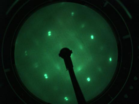
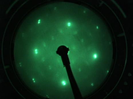
LEED Patterns
Annealed at 400 °C for 30 Seconds
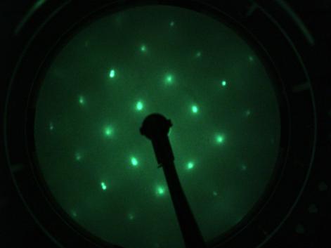 Ni (100) - LEED Pattern 90 eV at 400 °C
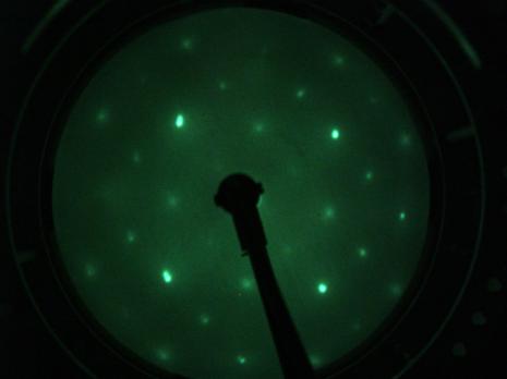 Ni (100) - LEED Pattern 110 eV at 400 °C
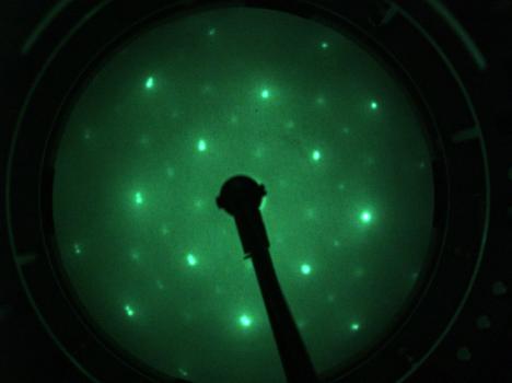 Ni (100) - LEED Pattern 210 eV at 400 °C
Annealed at 680 °C for 30 Seconds
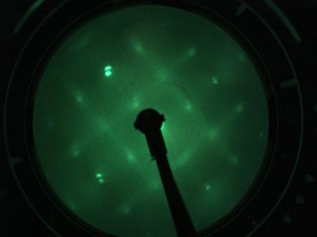 Ni (100) - LEED Pattern 90 eV at 680 °C
 Ni (100) - LEED Pattern 110 eV at 680 °C
 Ni (100) - LEED Pattern 210 eV at 680 °C
Ni 100 - AES Spectrum
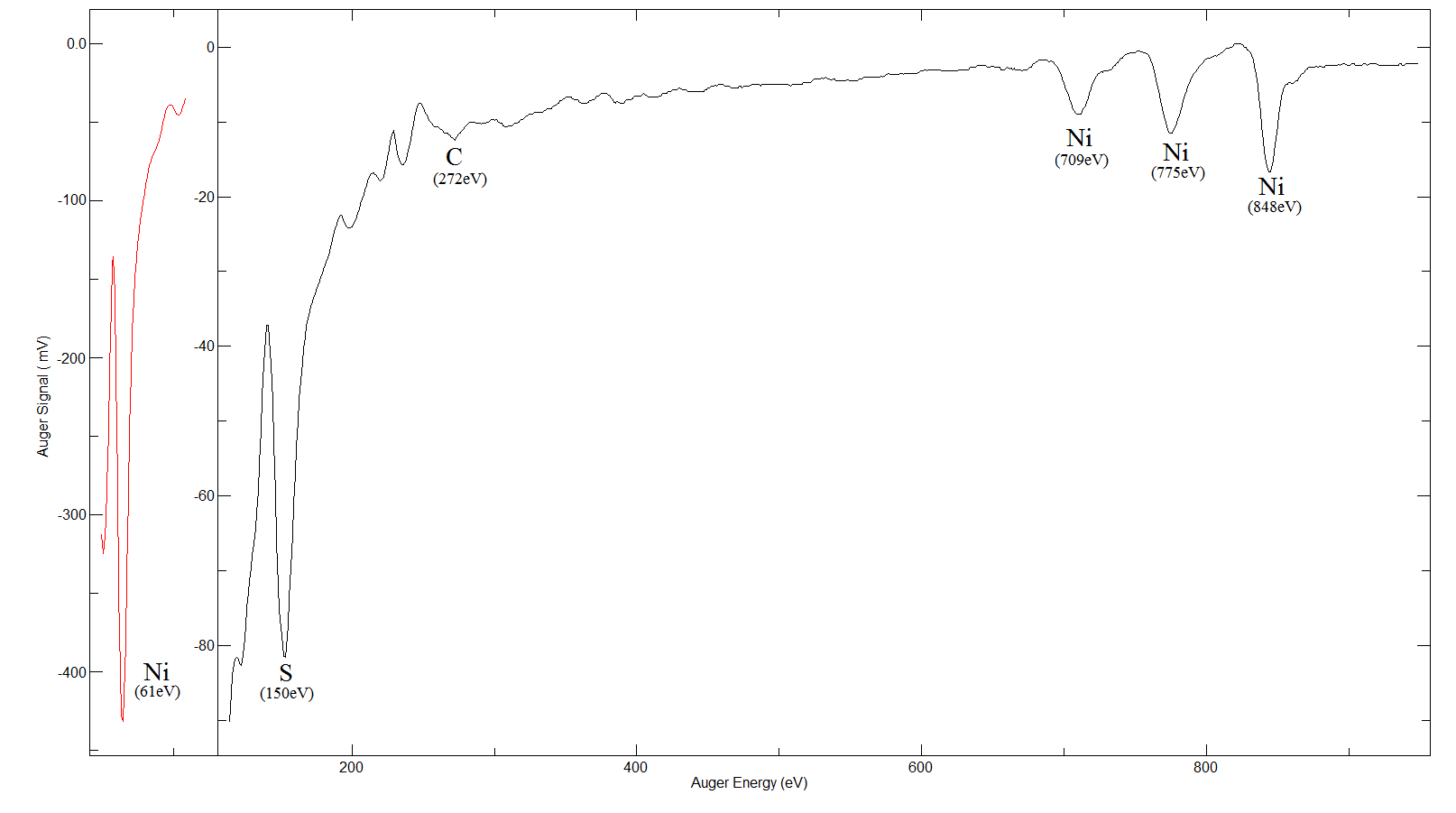 Ni 100 – AES Spectrum
Related Links