Low Energy Electron Diffraction & Auger Electron Spectroscopy Data
Epitaxial Films on Substrates > Ti / Ga2O3-β (010) - Titanium on Gallium Oxide
Specifications
- Material: Titanium on Gallium Oxide (010)
- Size: 5 × 5 × 0.5 mm
- Orientation: (010)
- Structure: Monoclinic
- Lattice Constant: a = 12.23 Å, b = 3.04 Å, c = 5.80 Å
- Type/Dopant: Undoped
- Film Growth Method: Molecular Beam Epitaxy
- Melting Temperature: 1900 °C
- Debye Temperature: 600 °C [Ref. 3]
- Surface Debye Temperature: Unpublished
- Characterization Tool: LEED-AES
- Model LEED 800
- UHV Treatment: Annealing at 570 °C (estimated tempe. of sample) for 5 minutes
- Applications: Emerging uses in sensors, power electronics and semiconductor electronics
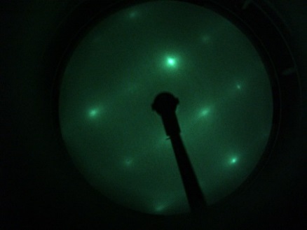
LEED Pattern - Ga2O3-β (010) with Ti (estimated layer thickness of 2.3nm) deposited onto the sample and annealed
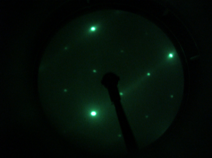 Ga2O3-β (010) - LEED Pattern 40 eV
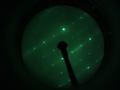 Ga2O3-β (010) - LEED Pattern 110 eV
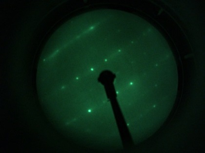 Ga2O3-β (010) - LEED Pattern 155 eV
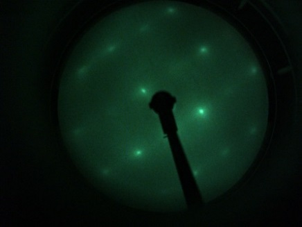
LEED Pattern - Ga2O3-β (010) with Ti (estimated layer thickness of 15.2nm) deposited onto the sample and annealed
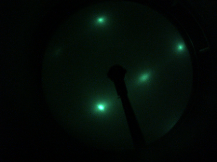 Ga2O3-β (010) - LEED Pattern 40 eV
 Ga2O3-β (010) - LEED Pattern 110 eV
 Ga2O3-β (010) - LEED Pattern 155 eV
Ti / Ga2O3-β with TI - AES Spectrum
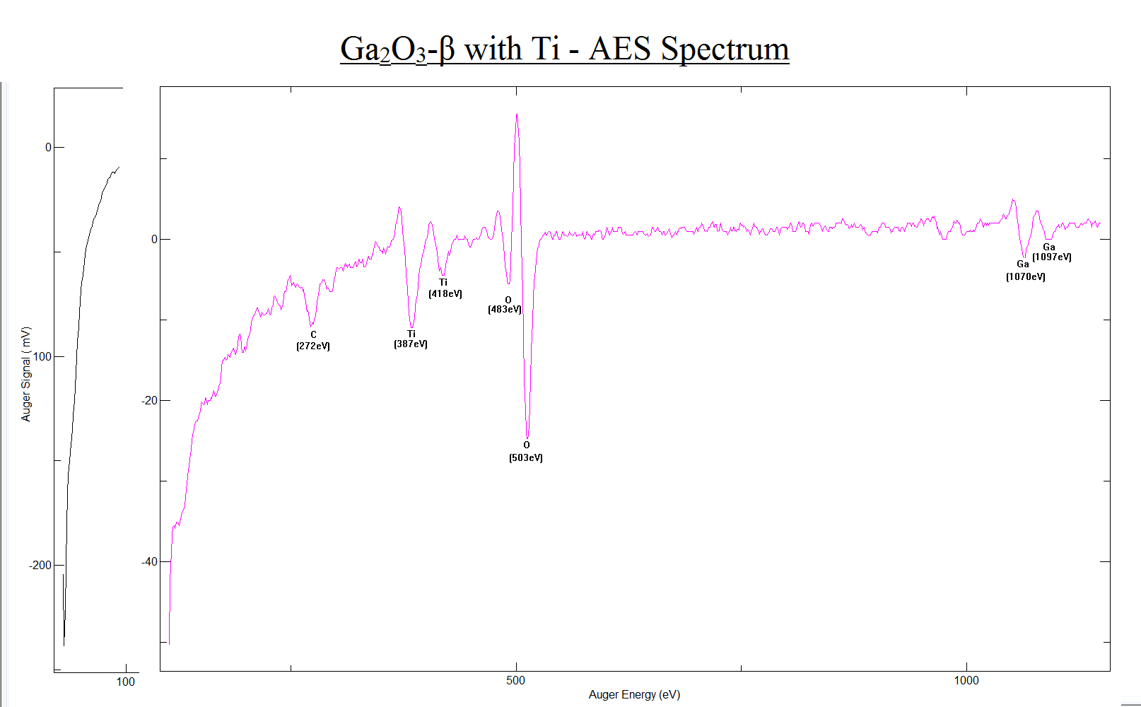 Estimated thickness of Ti: 2.3nm
Ti / Ga2O3-β with TI - AES Spectrum
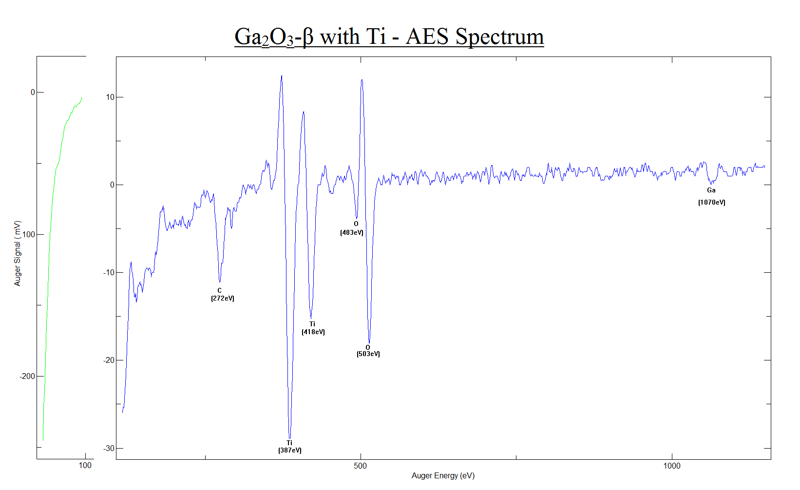 Estimated thickness of Ti: 15.2nm
Related Links