ocivm.com > LEED / AES Spectrometers > LEED 450 MAX MCP (Model BDL450-MAX-MCP) with Integral Retraction and Shutter
Upgraded version of the LEED450 featuring maximized display size for Surface crystallography.
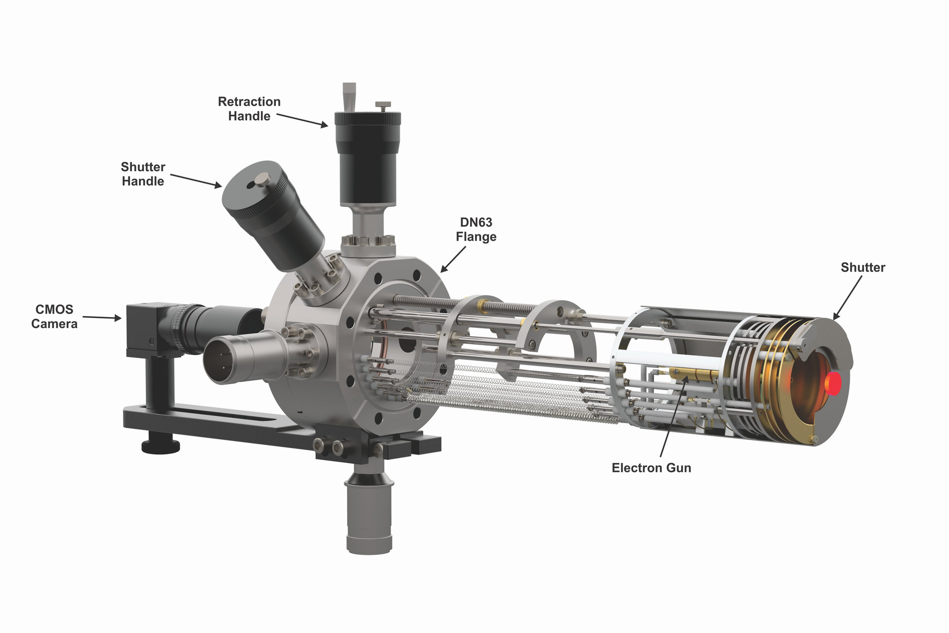 Figure 2. Model LPS075-D power supply for LEED operation.
 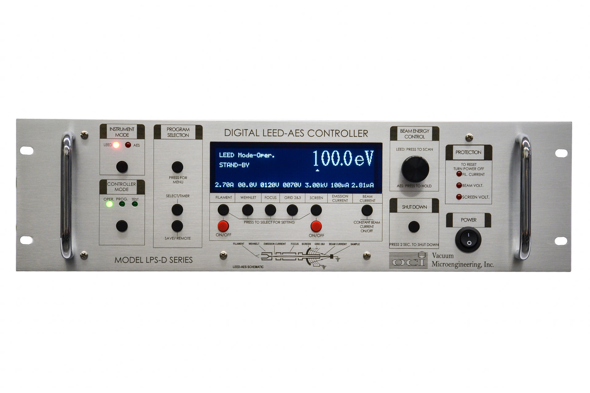 Figure 3. Model LPS300-D and LOA10-AES power supply for LEED and AES operation.
 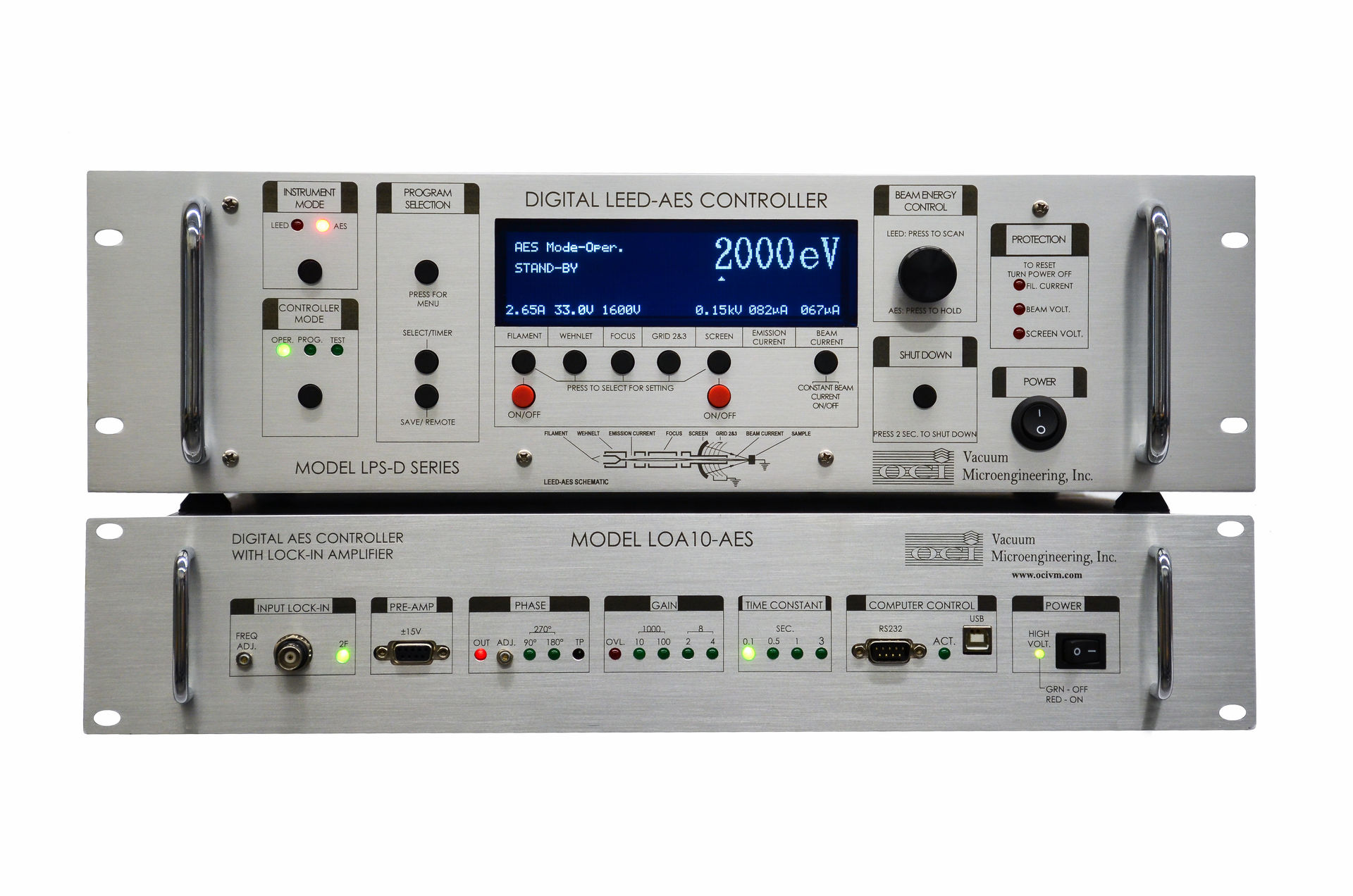 Figure 4. Model MCPS01/02 power supply for microchannel plate operation.
 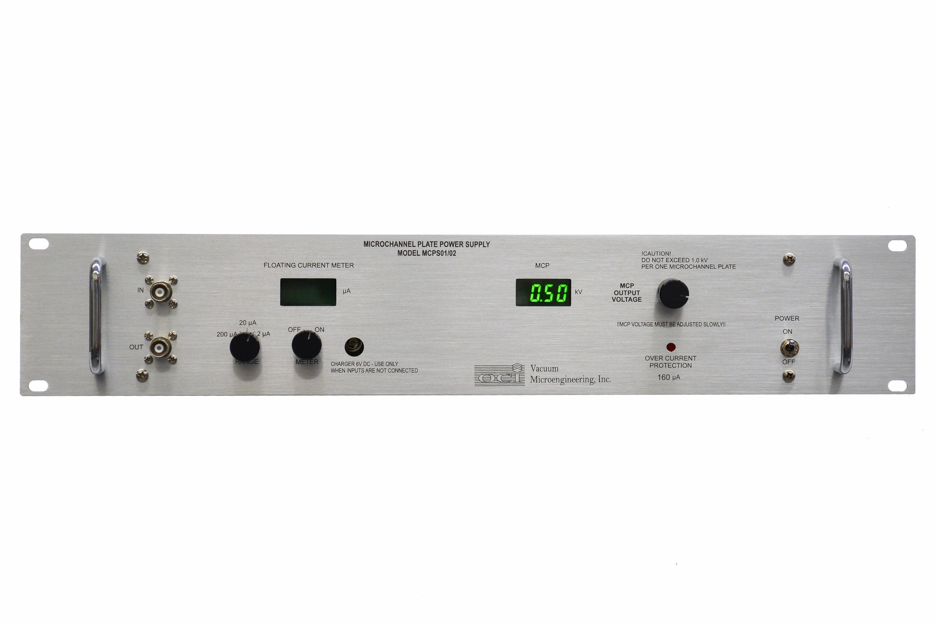 Figure 5. MultiLEED Software.
 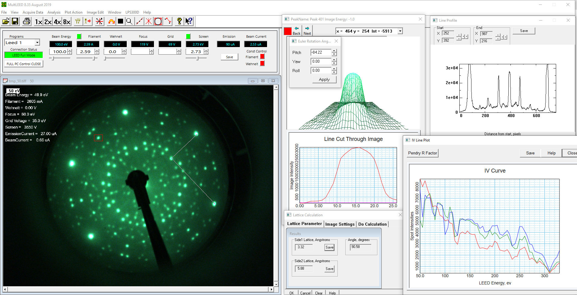 Figure 6. AES Software.
 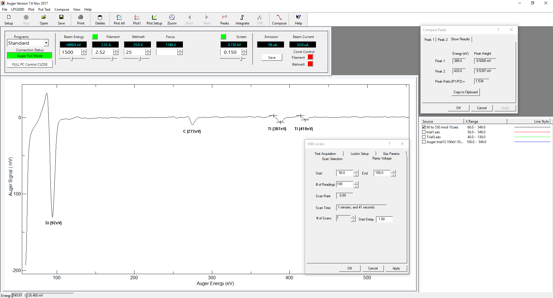 Figure 7. AES Software Images - element composition.
 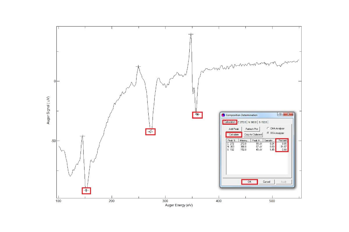 Figure 8. LEED pattern of Germanium (100) with 120 eV beam energy.
 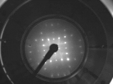 Figure 9. LEED pattern of Gallium Nitride (0001) with 64 eV beam energy.
 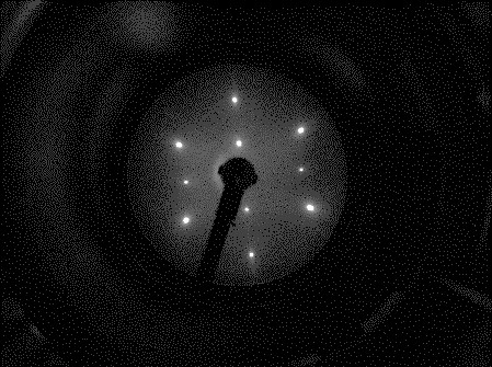 Figure 10. BP4 on Au (111) with 64 eV beam energy.
 -64eV.jpg) Figure 11. BP3 on Au (111) with 69 eV beam energy.
Figure 11. BP3 on Au (111) with 69 eV beam energy. -69eV.jpg) Figure 12. Auger spectrum of Gallium Nitride.
Figure 12. Auger spectrum of Gallium Nitride. 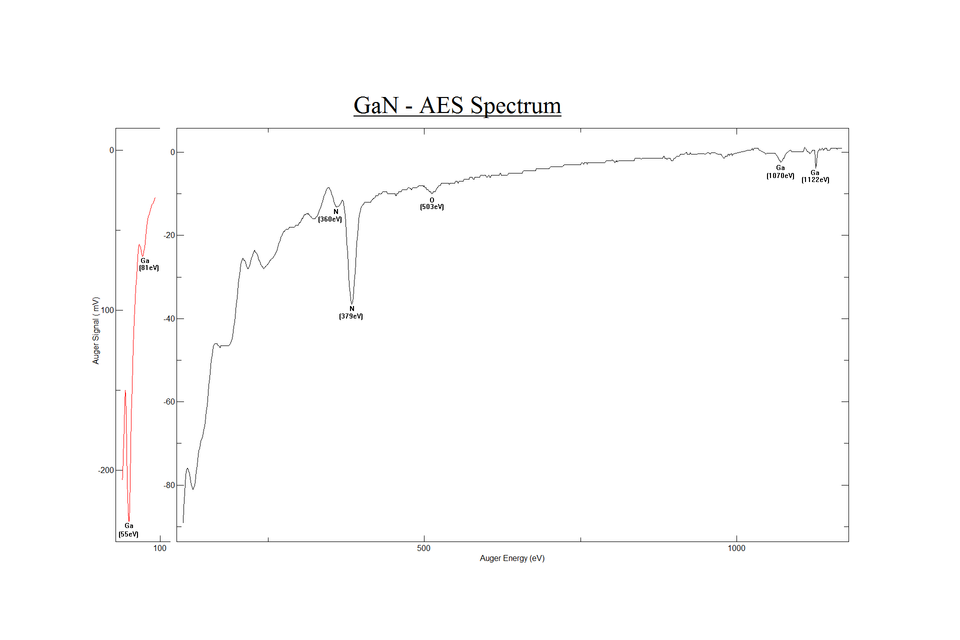 Figure 13. Auger spectrum of Gold.
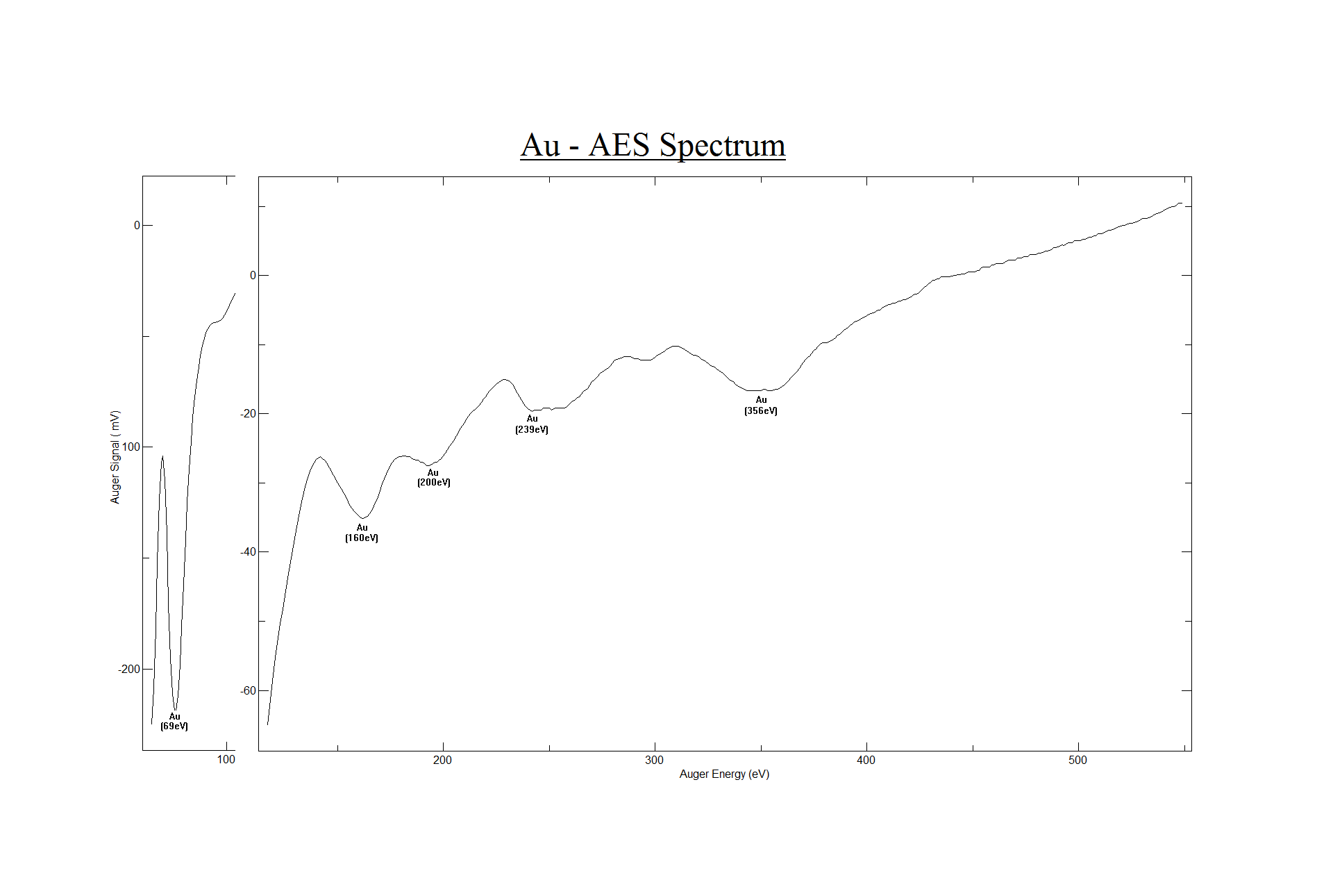
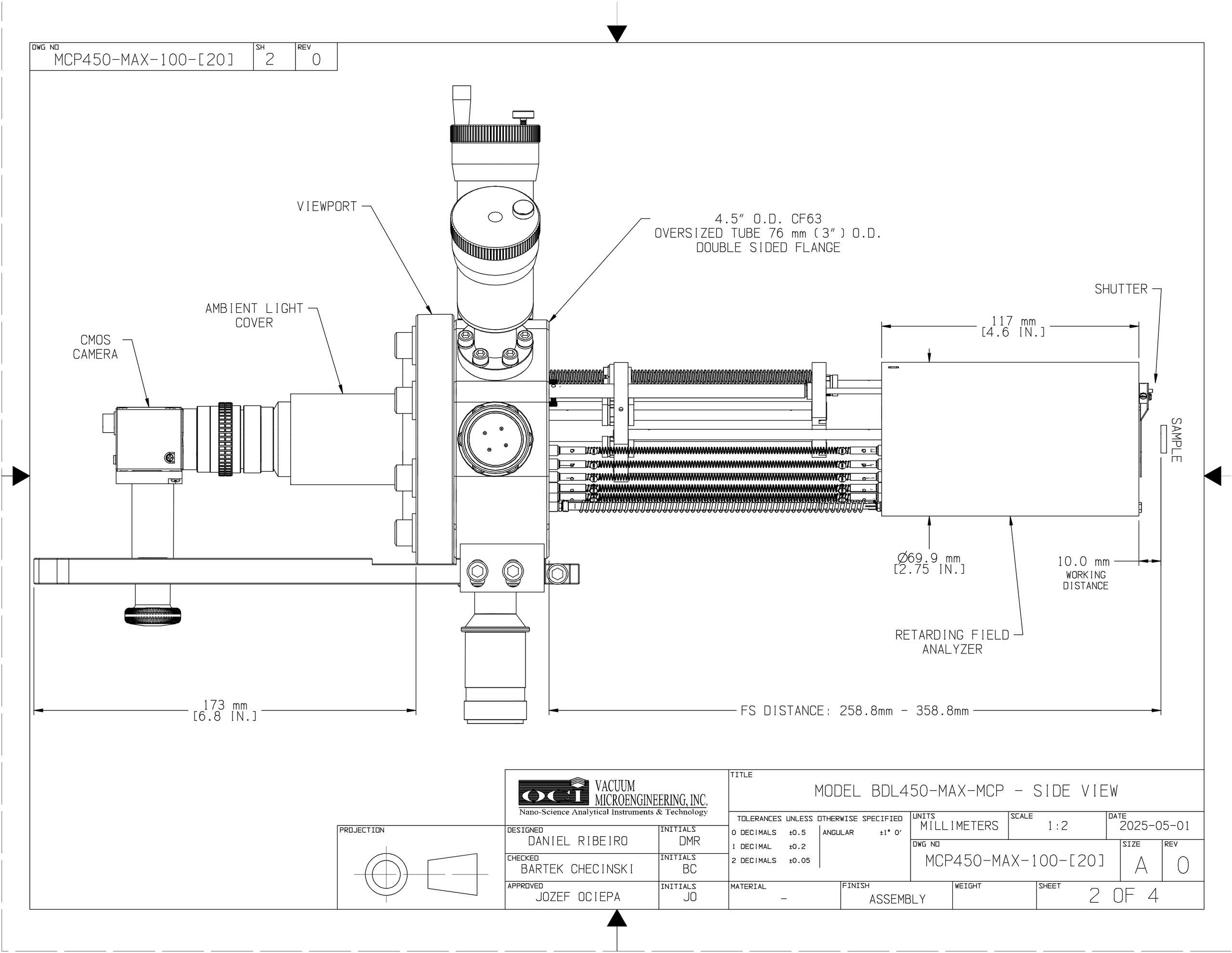
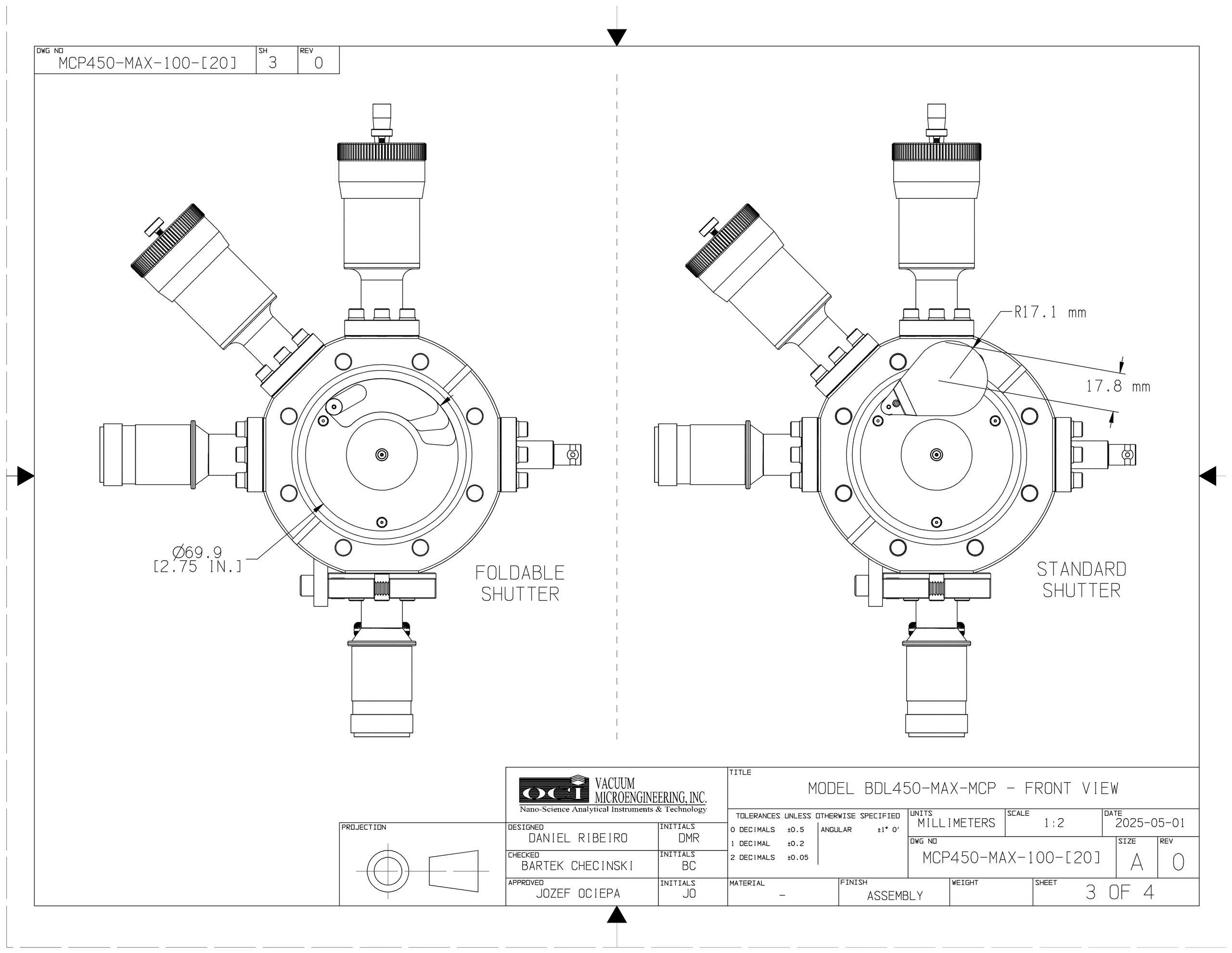
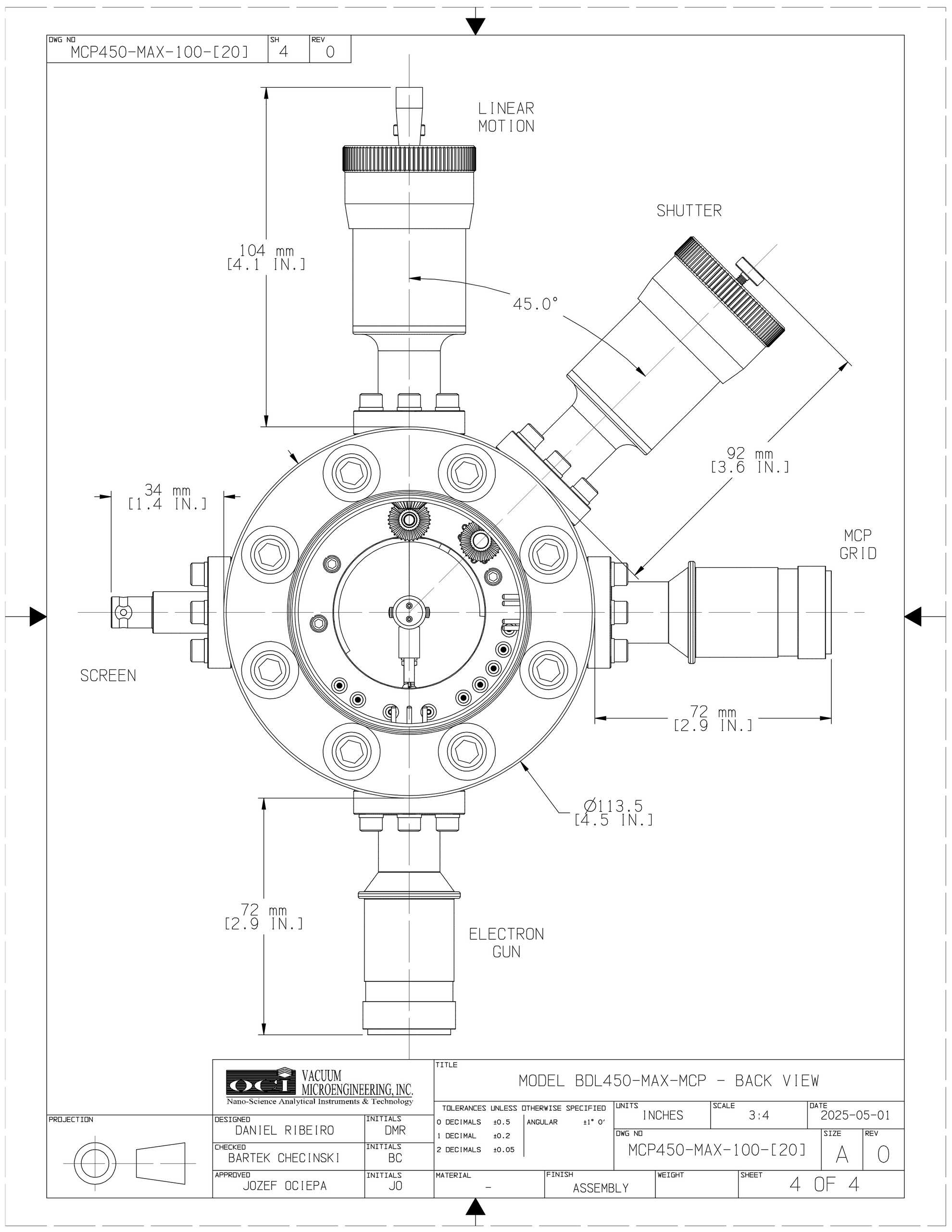
The LEED 450-MAX-MCP combines cutting-edge Low-Energy Electron Diffraction (LEED) and Auger Electron Spectroscopy (AES) capabilities. Featuring a miniature electron gun, a set of concentric grids, and a conductive, phosphor-coated screen, and the superior signal amplification of single microchannel plates (MCP). The MCP provide a high gain enabling the use of ultra-low beam currents to produce clear, high-resolution LEED patterns while minimizing sample damage—ideal for delicate materials like ice and organics.
Designed for ease of use, the LEED 450-MAX-MCP operates with a modern digital power supplies and a robust retraction mechanism, ensuring smooth, dependable day-to-day operation, as trusted by our extensive user base for decades. The wide viewing angle (60° at 37 mm sample distance) and minimal screen shadowing by the electron gun maximize the visible LEED pattern, providing unparalleled clarity and precision for surface science research.
Miniature model with maximized display for basic surface crystallography of single crystals and “in-situ” epitaxy.
The LEED 450 MAX-MCP is capable of providing LEED and AES data for a wide range of samples. The miniature instrument size allows for easy installation to smaller UHV systems.
Materials suitable for characterization should be single crystals and epitaxial films in categories such as: 2D materials, semiconductors, metals, oxides and magnetic films.
For seamless integration, 3D step files are available for most models on the PDF Downloads page.
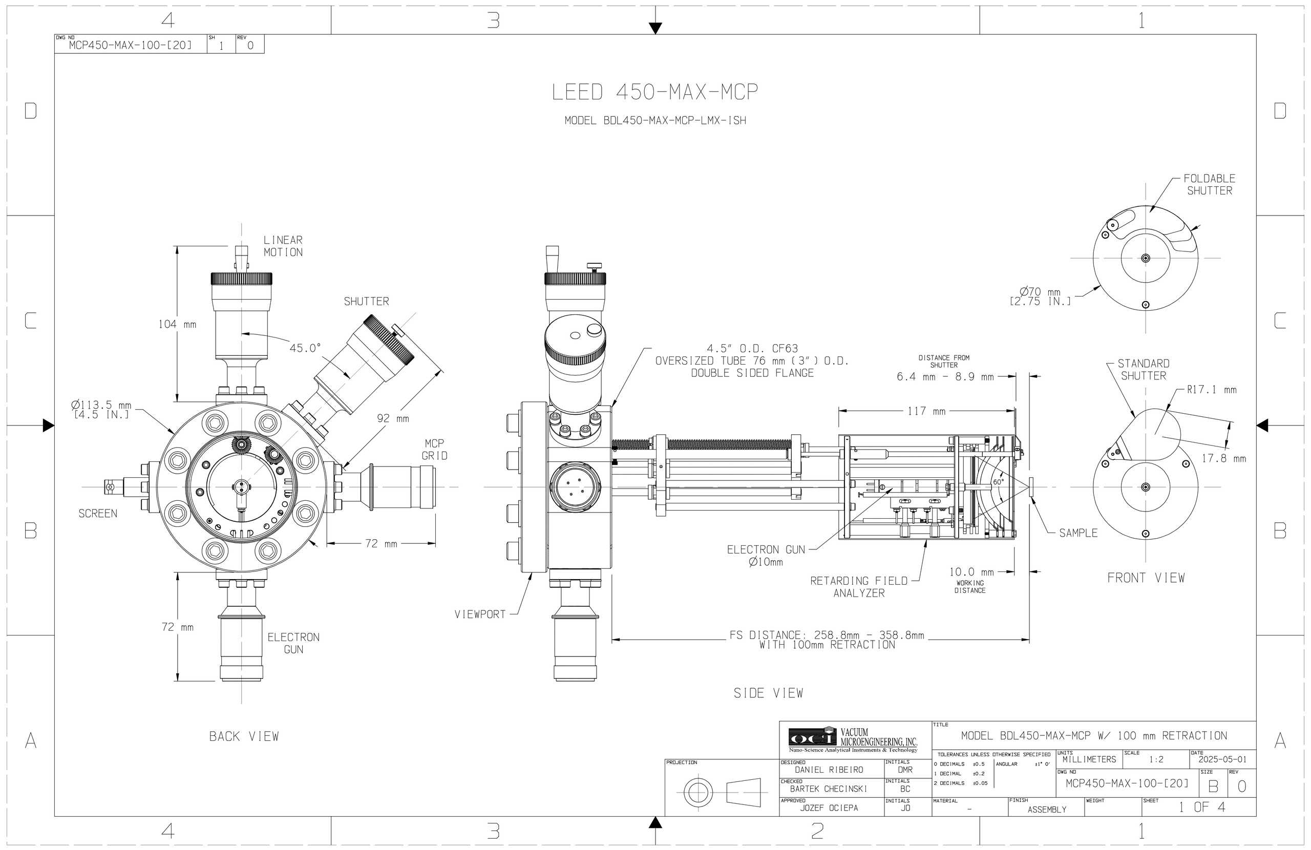
LEED 450 MAX MCP (Model BDL450-MAX-MCP) calculation formula for Flange-Sample distance
& Retraction length:
FS = 165.5mm + 2 LMX – OV; where FS is the flange to sample distance, LMX is the retraction
length and OV is the overlapping length.
For detailed specifications, download LEED 450 MAX MCP Specifications (.pdf).
| Optics | |
|---|---|
| Glass-display | Fused silica coated with indium-tin oxide conductive layer and P31 phosphor (ZnS:Ag:Cu-green, 525 nm wavelength) |
| Acceptance angle | 60° angle of acceptance from sample at a distance of 37 mm |
| Retarding Field Analyser | Concentric assembly of hemispherical grids |
| Working distance | 10 mm from sample |
| Grid material | Gold coated St-Steel wire mesh (100 mesh, 81% transparency) |
| Energy Resolution | 0.2% - 0.5% at low modulation voltages |
| Monitoring | 4.5 " standard viewport |
| Linear motion | up to 100 mm retraction from sample; linear ball bearing and acme thread with all spring electr. connections |
| Integral Shutter | Manual shutter driven by rotary feedthrough |
| Magnetic shielding | Mu-metal cylinder with front cover for maximum attenuation |
| Assembly | Extreme-high-vacuum compatibility with stainless steel, high alumina and Au-plated copper alloy materials |
| Mounting | CF4.5" (DN63CF) With Oversized tubing 76 mm (3”) O.D |
| Bakeability | Under vacuum, 250 °C maximum |
| Integral Miniature Electron Gun | |
| Beam energy system | LEED – 5 eV to 750 eV, AES – 5 eV to 3000 eV |
| Beam current | LEED – 2 μA at 100 eV and 0.5 mm beam size, AES - up to 100 μA at 3 keV |
| Beam size | from 1 mm to 250 μm - adjusted by Wehnelt potential, limited by exchangeable aperture down to 50 μm |
| Electron source | Tungsten-2% thoriated filament standard, single crystal LaB6 filament optional |
| Energy spread | 0.45 eV (thoriated - tungsten filament) |
| Overall size | 10 mm lens diameter and 80 mm length |
| Working area | 41 mm |
| L/D ratio | 40:1 |
| Channel diameter | 12 microns |
| Center to center spacing | 15 microns |
| Plate thickness | 0.48 mm |
| Bias angle | 8° |
| Electron gain | 104 to 105 per plate |
Download LEED 450-MAX-MCP Configuration Guide (.pdf).