LEED / AES Spectrometers
AES Models
Related
LEED-AES Models
IntegraLEED Surface Crystallography Spectrometer
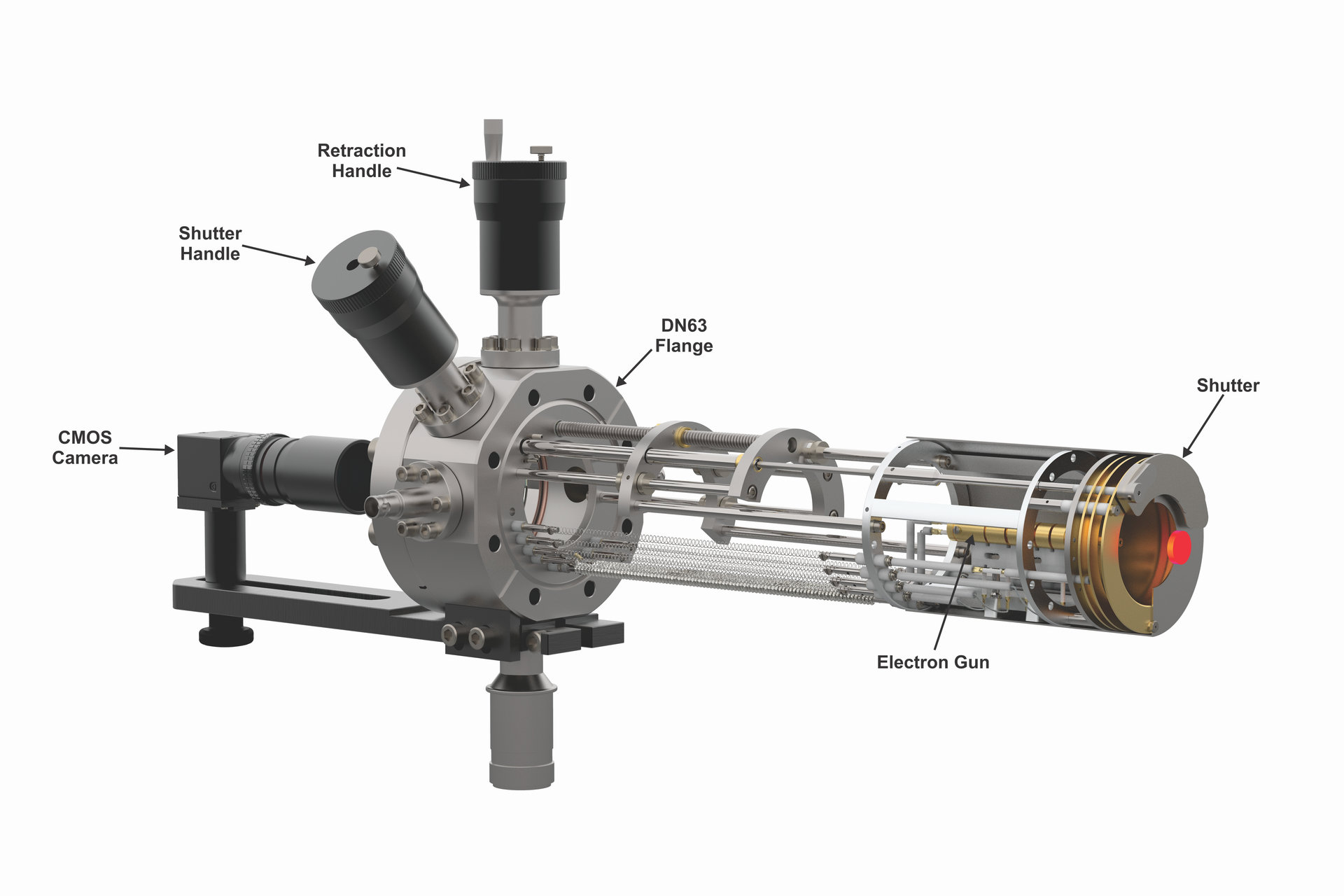
LEED 800 (Model BDL800IR) with Integral Retraction and Shutter
Full Flange Size LEED for Higher Angular and Energy Resolution
Based on Low Energy Electron Diffraction (LEED) and Auger Spectroscopy (AES)
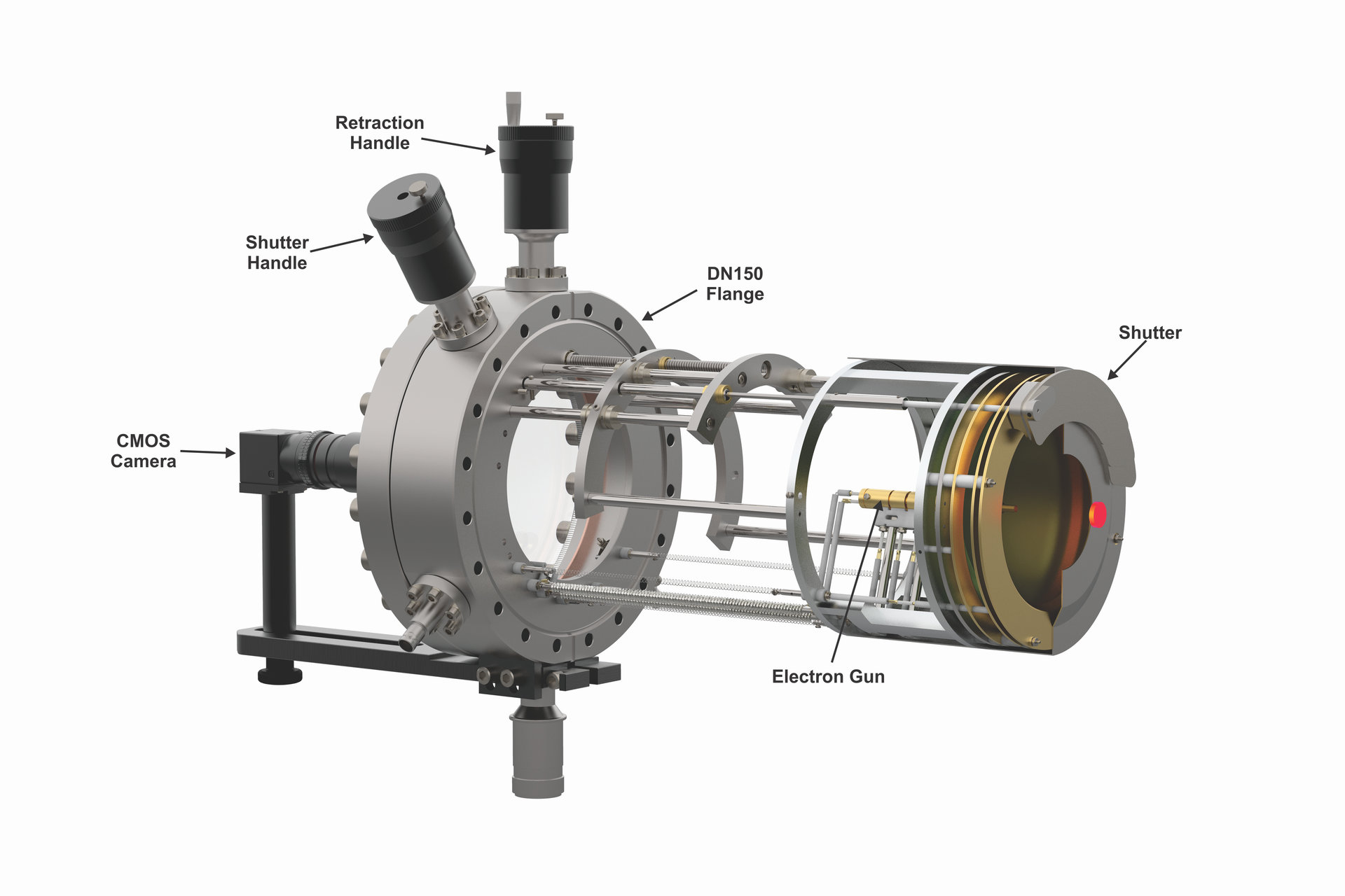 Figure 2. Model LPS075-D power supply for LEED operation.
  Figure 3. Model LPS300-D and LOA10-AES power supply for LEED and AES operation.
  Figure 4. MultiLEED Software.
 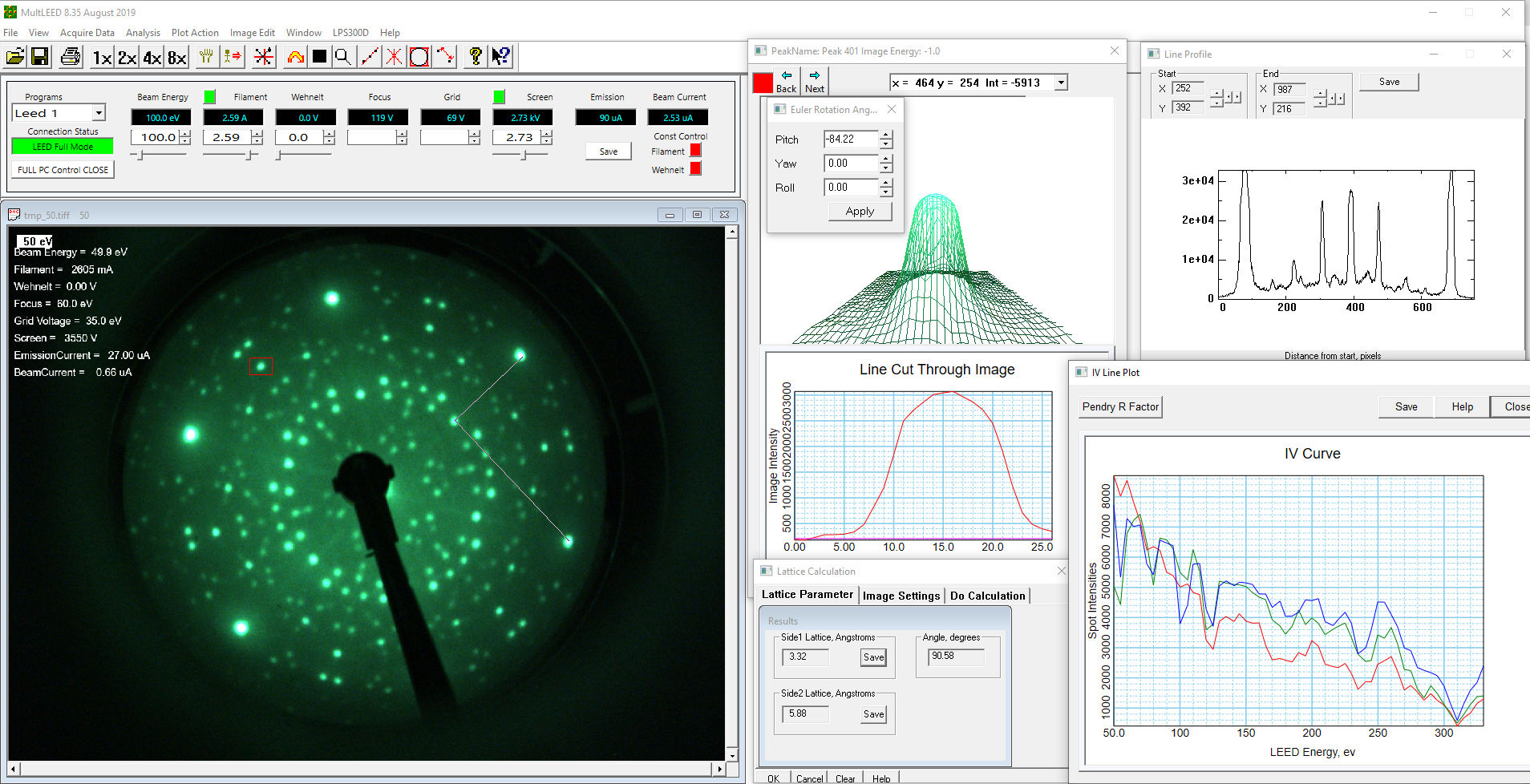 Figure 5. AES Software.
 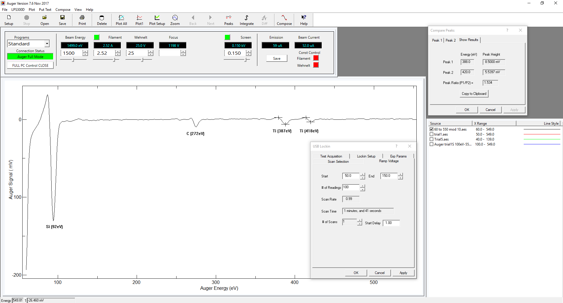 Figure 6. AES Software Images - element composition.
  Figure 7. LEED pattern of a Silicon (111) sample with 120 eV beam energy.
 -120_eV.jpg) Figure 8. LEED pattern of Strontium Titanate (100) with 95 eV beam energy.
Figure 8. LEED pattern of Strontium Titanate (100) with 95 eV beam energy. -95_eV.jpg) Figure 9. LEED pattern of Silicon Carbide 6H (0001) with Titanium (estimated deposited layer thickness of 56.0mm) with 130 eV beam energy.
Figure 9. LEED pattern of Silicon Carbide 6H (0001) with Titanium (estimated deposited layer thickness of 56.0mm) with 130 eV beam energy. -130_eV.jpg) Figure 10. LEED pattern of Yttrium Iron Garnet with 15 eV beam energy.
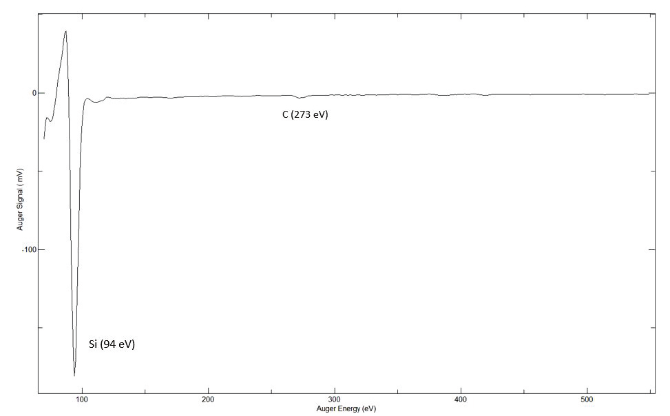
Figure 10. LEED pattern of Yttrium Iron Garnet with 15 eV beam energy. 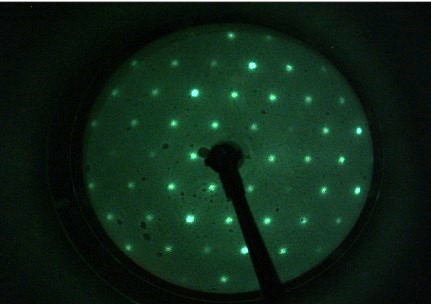 Figure 11. Auger Spectrum of Silicon Carbide 6H with Titanium.
 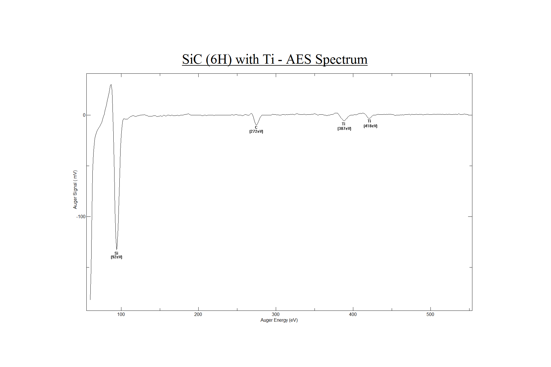 Figure 12. Auger spectrum of Yttrium Iron Garnet.
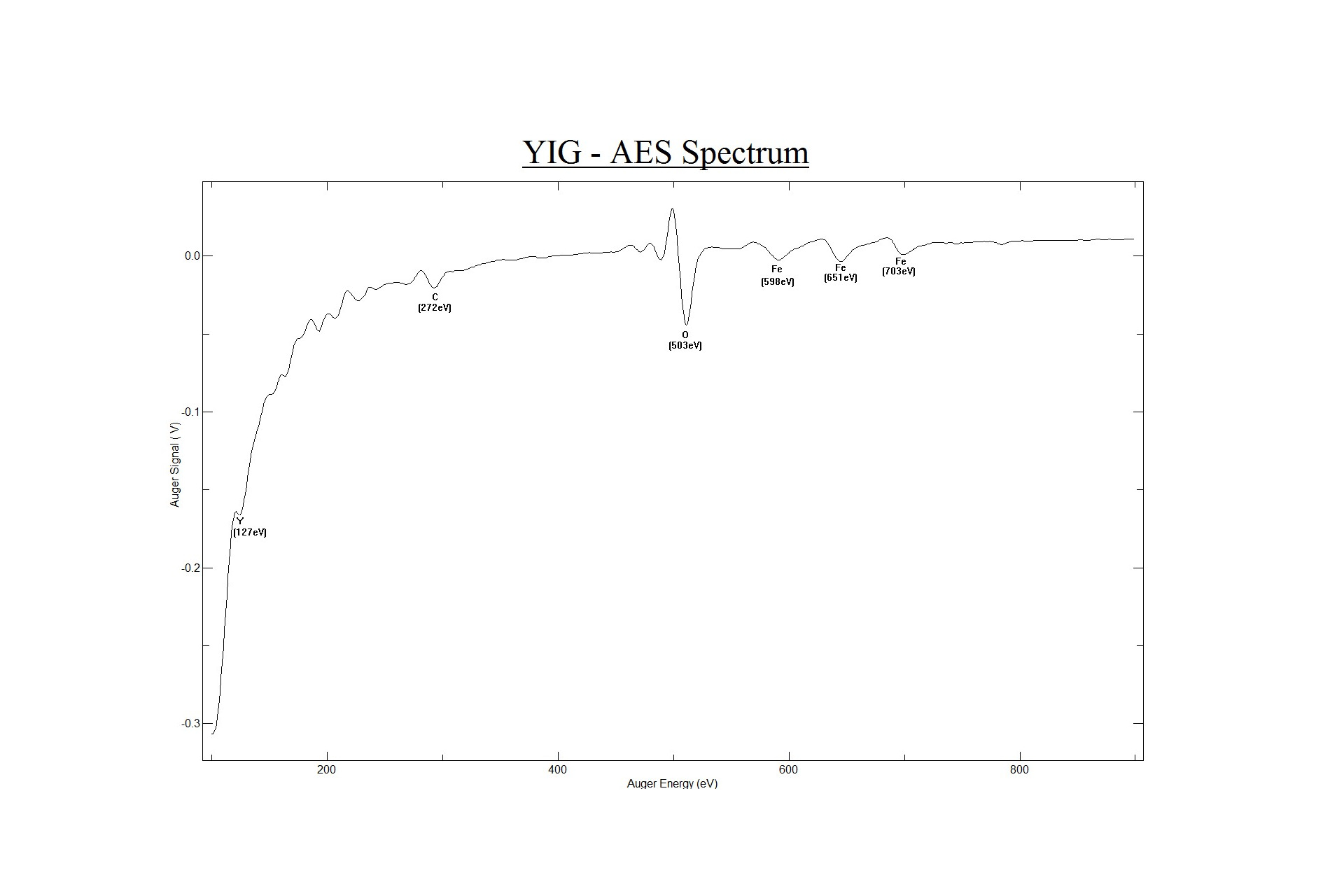
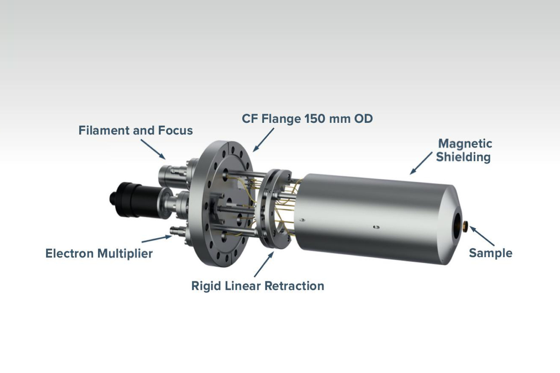
The LEED 800 combines cutting-edge Low-Energy Electron Diffraction (LEED) and Auger Electron Spectroscopy (AES) capabilities in a compact, reliable package. Featuring a miniature electron gun, a set of concentric grids, and a conductive, phosphor-coated screen, this high-performance instrument delivers exceptionally sharp and bright LEED patterns with outstanding resolution in k-space (typical transfer width of 300 Å at 100 eV).
Designed for ease of use, the LEED 800 operates with a modern digital power supply and a robust retraction mechanism, ensuring smooth, dependable day-to-day operation, as trusted by our extensive user base for decades. The wide viewing angle (100 ° at 75 mm sample distance) and minimal screen shadowing by the electron gun maximize the visible LEED pattern, providing unparalleled clarity and precision for surface science research.
For details, visit the LEED 800 Product Page.
Features
- High energy & image resolution for LEED and AES with no Moire pattern interference
- Large angle (100 °) fluorescent LEED display and superior magnetic shielding
- Miniature electron gun with large coherence width and dual lenses
- Suitable for in-situ film growth monitoring
- Low outgassing rate
- Convenient LEED image Capture with external camera
- Simple and powerful operation with digital controller
Specifications, Configuration and More
IntegraLEED-Surface Crystallography Spectrometer
LEED600 (Model BDL600) with Integral Retraction and Shutter
Compact LEED to Fit Smaller UHV Systems
Based on Low Energy Electron Diffraction (LEED) and Auger Spectroscopy (AES)
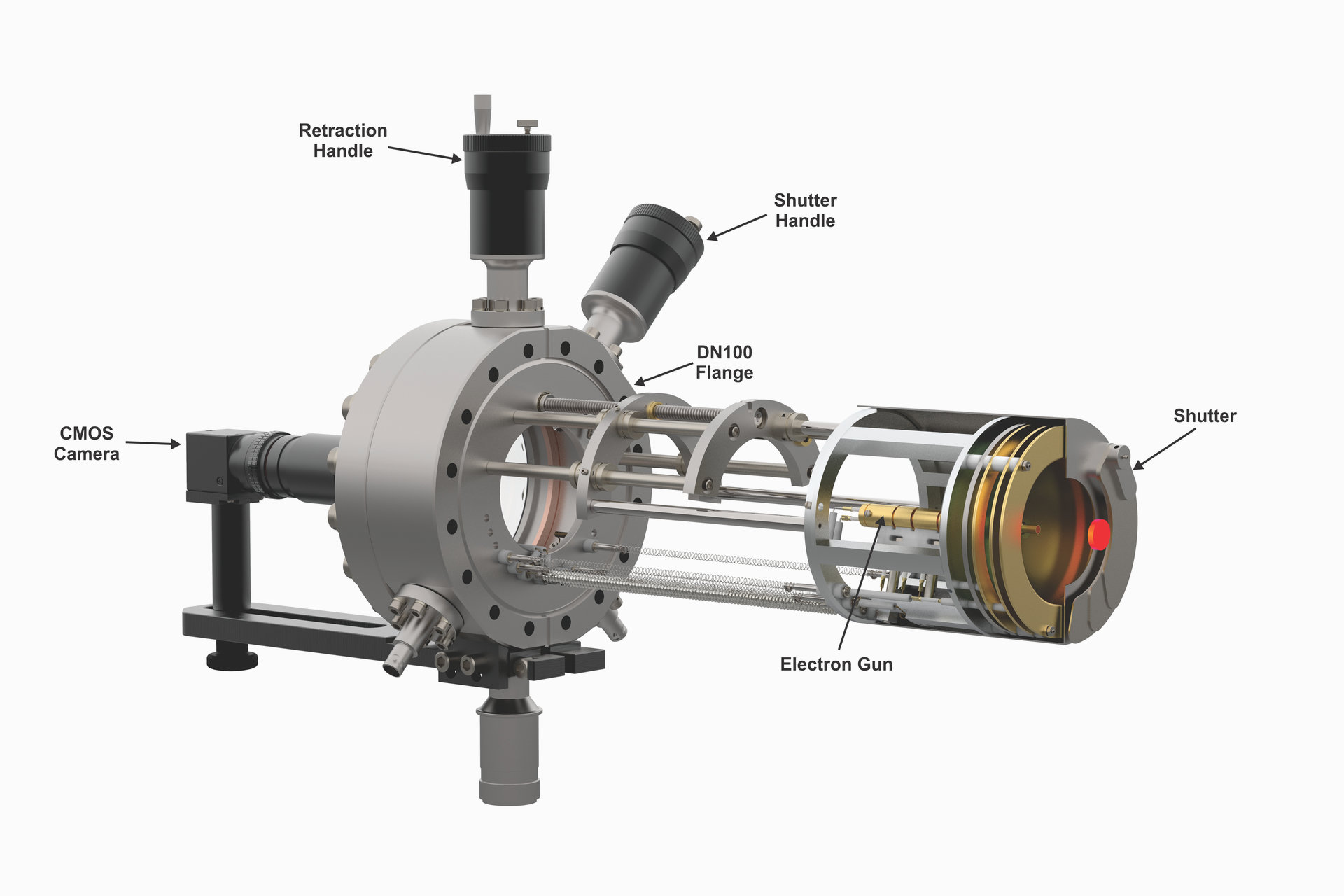 Figure 2. Model LPS075-D power supply for LEED operation.
 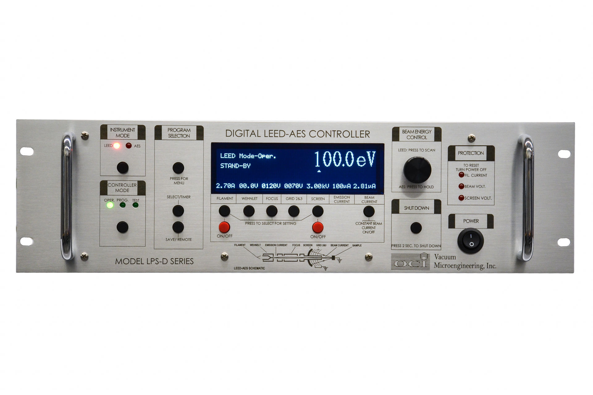 Figure 3. Model LPS300-D and LOA10-AES power supply for LEED and AES operation.
  Figure 4. MultiLEED Software.
Figure 5. AES Software.
Figure 6. AES Software Images - element composition.
Figure 4. MultiLEED Software.
Figure 5. AES Software.
Figure 6. AES Software Images - element composition.  Figure 7. LEED pattern of Komori Si(111) t51 sample.
 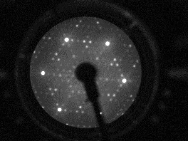 Figure 8. Ni (100): a) 110 eV b) O2 reconstruction c) H2 reconstruction.
 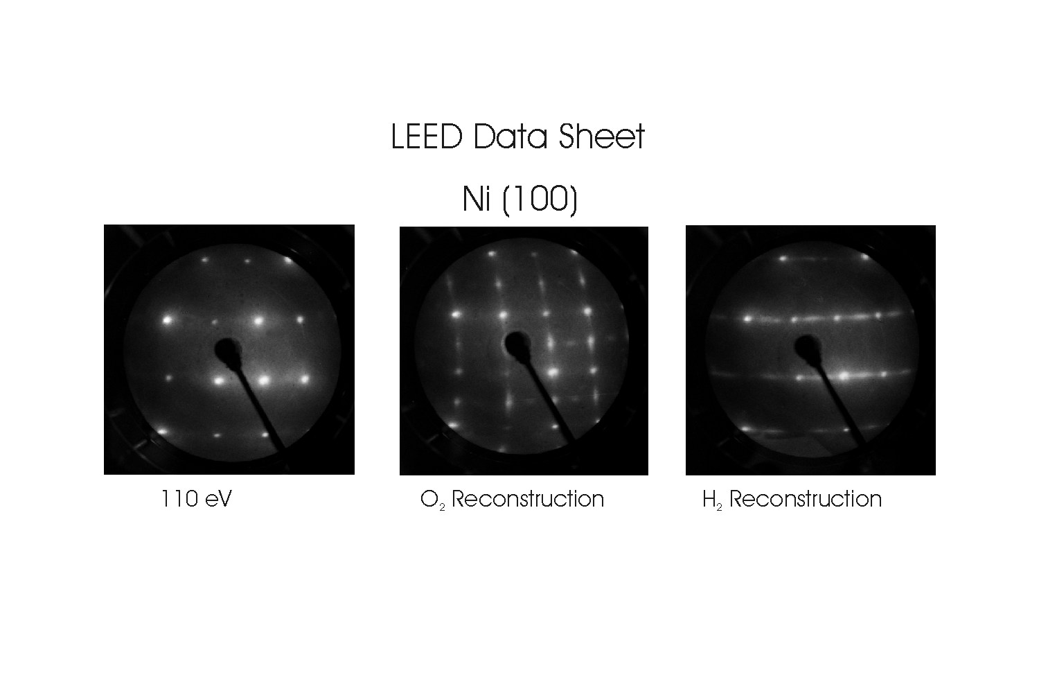 Figure 9. Auger spectrum of Iron (thick layer) on Magnesium Oxide.
 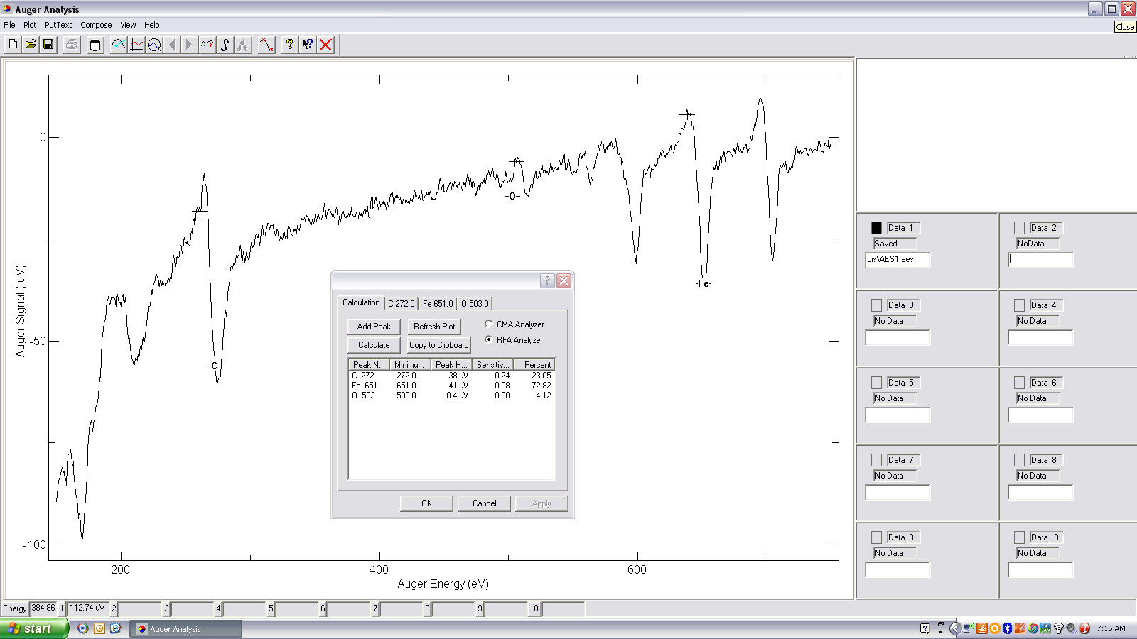 Figure 10. Auger spectrum of Silicon (111).
Description
The LEED 600 combines cutting-edge Low-Energy Electron Diffraction (LEED) and Auger Electron Spectroscopy (AES) capabilities in a compact, reliable package. Featuring a miniature electron gun, a set of concentric grids, and a conductive, phosphor-coated screen, this high-performance instrument delivers exceptionally sharp and bright LEED patterns.
Designed for ease of use, the LEED600 operates with a modern digital power supply and a robust retraction mechanism, ensuring smooth, dependable day-to-day operation, as trusted by our extensive user base for decades. The wide viewing angle (93 ° at 50 mm sample distance) and minimal screen shadowing by the electron gun maximize the visible LEED pattern, providing unparalleled clarity and precision for surface science research.
Features
- High energy & image resolution for LEED and AES with no Moire pattern interference
- Large Angle (93 °) fluorescent LEED display and superior magnetic shielding
- Miniature electron gun with large coherence width and dual lenses
- Suitable for in-situ film growth monitoring
- Low outgassing rate
- Convenient LEED image capture with external camera
- Simple and powerful operation with digital controller
Specifications, Configuration and More
IntegraLEED Surface Crystallography Spectrometer
LEED450-MAX(Model BDL450-MAX) with Integral Retraction and Shutter
Miniature Instrument to Fit Any UHV System
Upgraded version of the LEED450 featuring maximized display size for Surface crystallography
The LEED450-MAX combines cutting-edge Low-Energy Electron Diffraction (LEED) and Auger Electron Spectroscopy (AES) capabilities in a compact, reliable package. Featuring a miniature electron gun, a set of concentric grids, and a conductive, phosphor-coated screen, this high-performance instrument delivers exceptionally sharp and bright LEED patterns.
Designed for ease of use, the LEED450-MAX operates with a modern digital power supply and a robust retraction mechanism, ensuring smooth, dependable day-to-day operation, as trusted by our extensive user base for decades. The wide viewing angle (92° at 38 mm sample distance) and minimal screen shadowing by the electron gun maximize the visible LEED pattern, providing unparalleled clarity and precision for surface science research.
Features
- Sufficient angular and energy resolution to detect surface reconstructions and composition changes
- Miniature electron gun with double focusing
- Superior magnetic shielding
- Moiré pattern reduction
- Suitable for "in situ" growth monitoring
- Integral linear motion and shutter
- Low outgassing rate
- Easy add-on AES
- Convenient LEED image Capture with external camera
- Simple and powerful operation with digital controller
Specifications, Configuration and More
IntegraLEED-Surface Crystallography Spectrometer
LEED450(Model BDL450) w. External Retraction and Internal Shutter
Miniature Instrument to Fit Any UHV System
Based on Low Energy Electron Diffraction (LEED) and Auger Spectroscopy (AES)
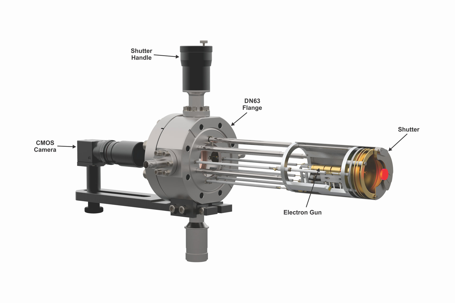 Figure 2. Model LPS075-D power supply for LEED operation.
  Figure 3. Model LPS300-D and LOA10-AES power supply for LEED and AES operation.
  Figure 4. MultiLEED Software.
  Figure 5. AES Software.
  Figure 5. AES Software Images - element composition.
 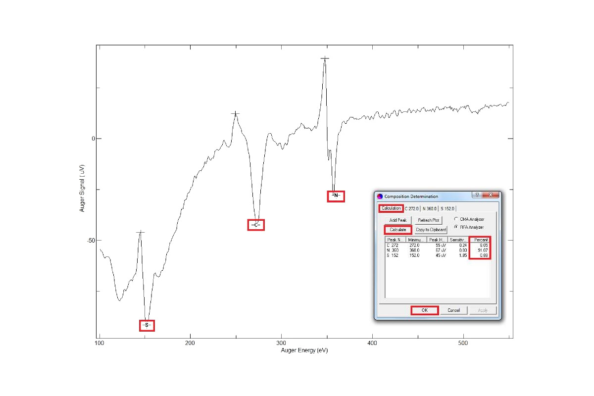 Figure 6. LEED pattern of a CuAl (111) sample with 125 eV beam energy.
 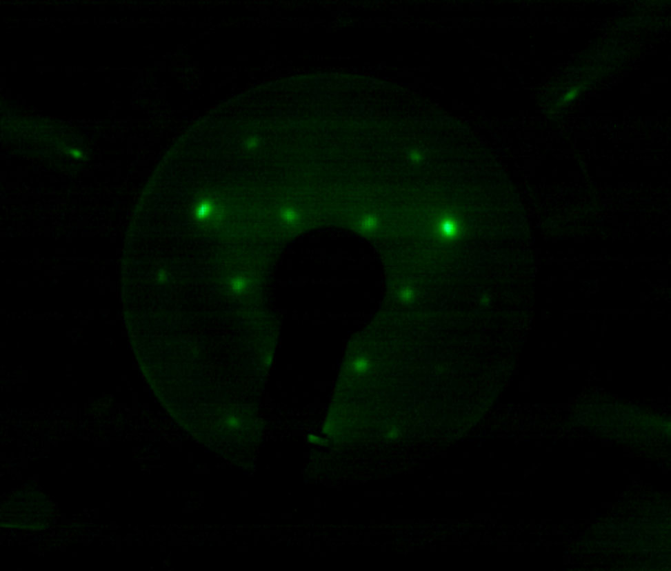 Figure 7. LEED pattern of CuAl (111) with 108 eV beam energy.
 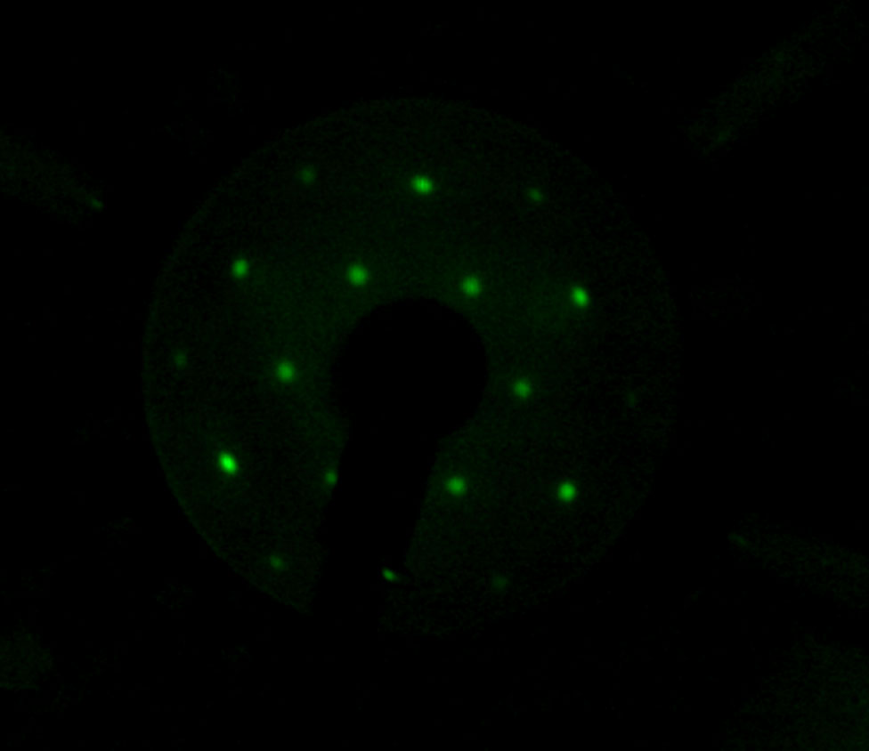 Figure 8. LEED pattern of CuAl (111) with 22-108 eV beam energy.
 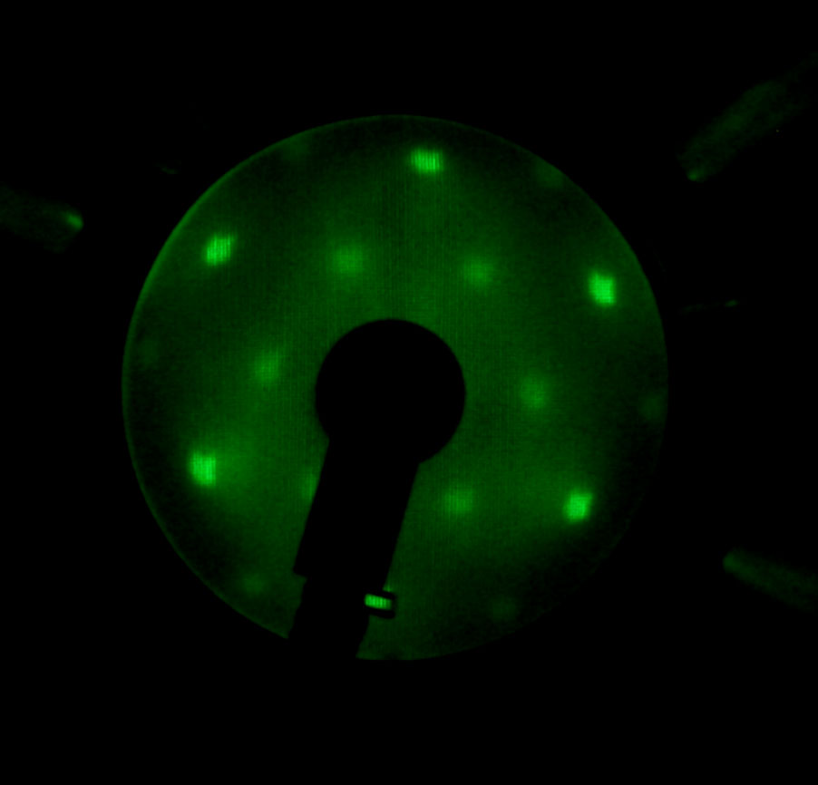 Figure 9. EED pattern of Graphene on Iridium (111) with 74 eV beam energy.
 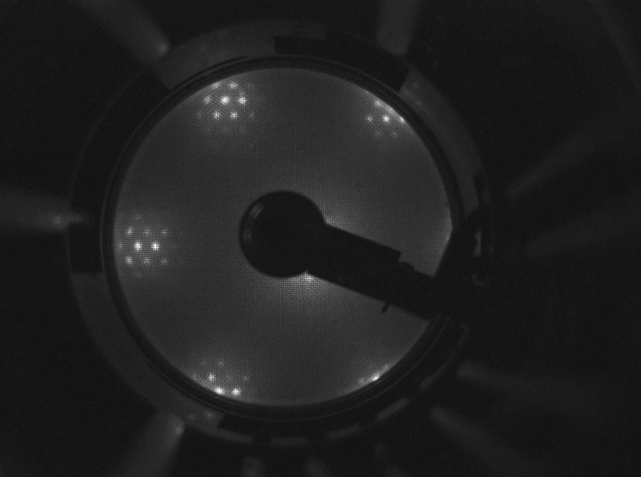 Figure 10. Auger spectrum of TiO2.
 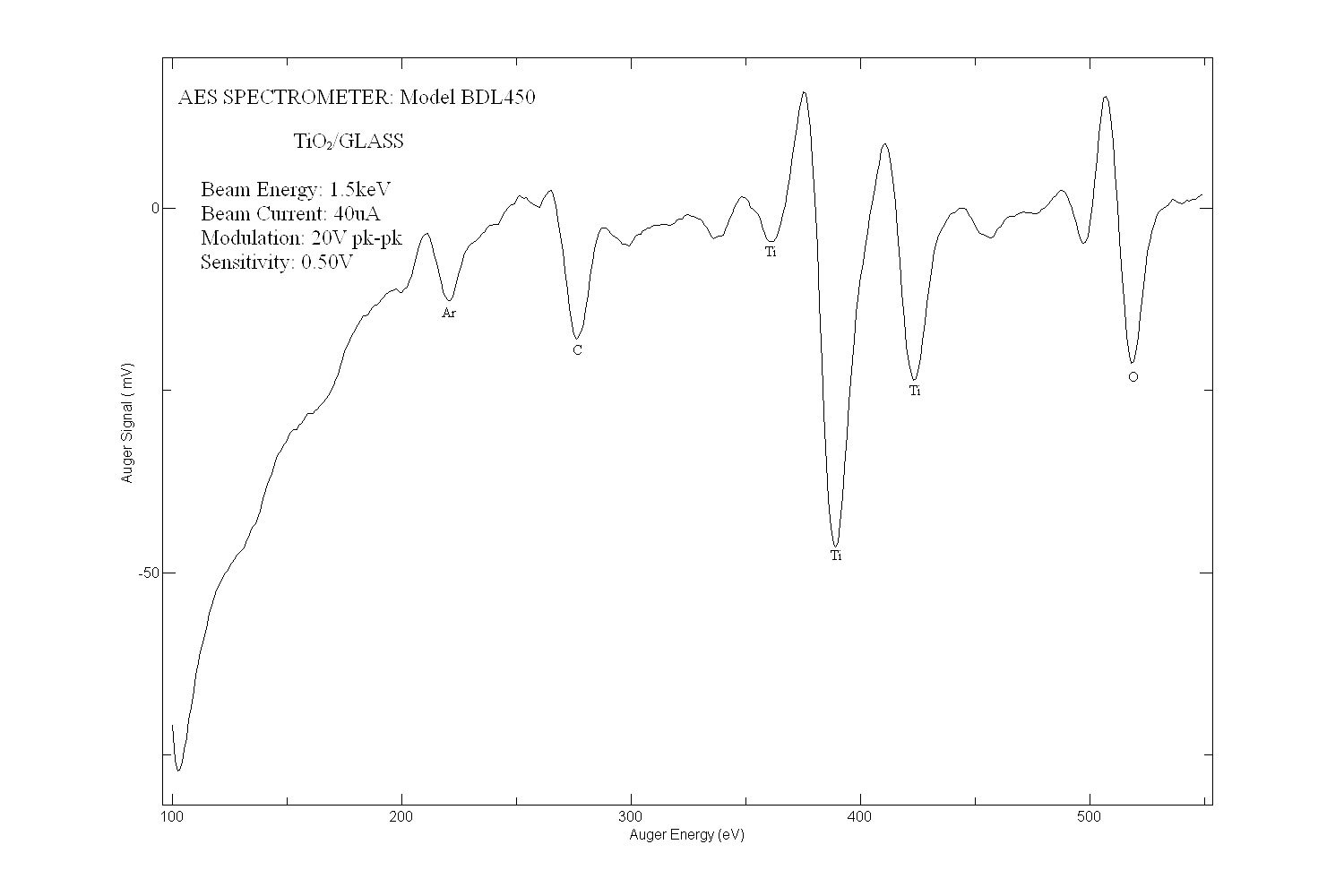 Figure 11. Auger spectrum of SrTiO3.
 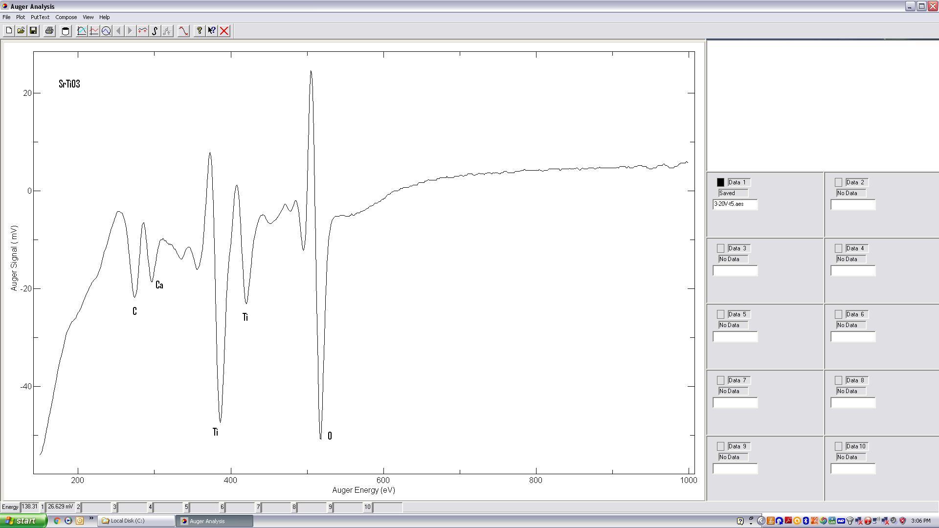 -->
-->
The LEED 450 combines cutting-edge Low-Energy Electron Diffraction (LEED) and Auger Electron Spectroscopy (AES) capabilities in a mini, reliable package. Featuring a miniature electron gun, a set of concentric grids, and a conductive, phosphor-coated screen, this high-performance instrument delivers exceptionally sharp and bright LEED patterns.
Designed for ease of use, the LEED 450 operates with a modern digital power supply and a robust retraction mechanism, ensuring smooth, dependable day-to-day operation, as trusted by our extensive user base for decades. The wide viewing angle (83 ° at 34mm sample distance) and minimal screen shadowing by the electron gun maximize the visible LEED pattern, providing unparalleled clarity and precision for surface science research.
Features
- Large Angle (83 °) Fluorescent LEED Display and superior magnetic shielding
- Miniature electron gun with large coherence width and dual lenses
- Suitable for In Situ Film Growth Monitoring
- Low outgassing rate
- Convenient LEED Image Capture with External Camera
- Simple and Powerful Operation with Digital Controller
Specifications, Configuration and More
LEED-AES Models w. MCP
IntegraLEED Surface Crystallography Spectrometer
Based on Low Energy Electron Diffraction (LEED) and Auger Spectroscopy (AES)
LEED 800 MCP 100DEG (Model BDL800IR-MCP-100DEG) with integral retraction and shutter
Organic Films & Molecular Beam Epitaxy
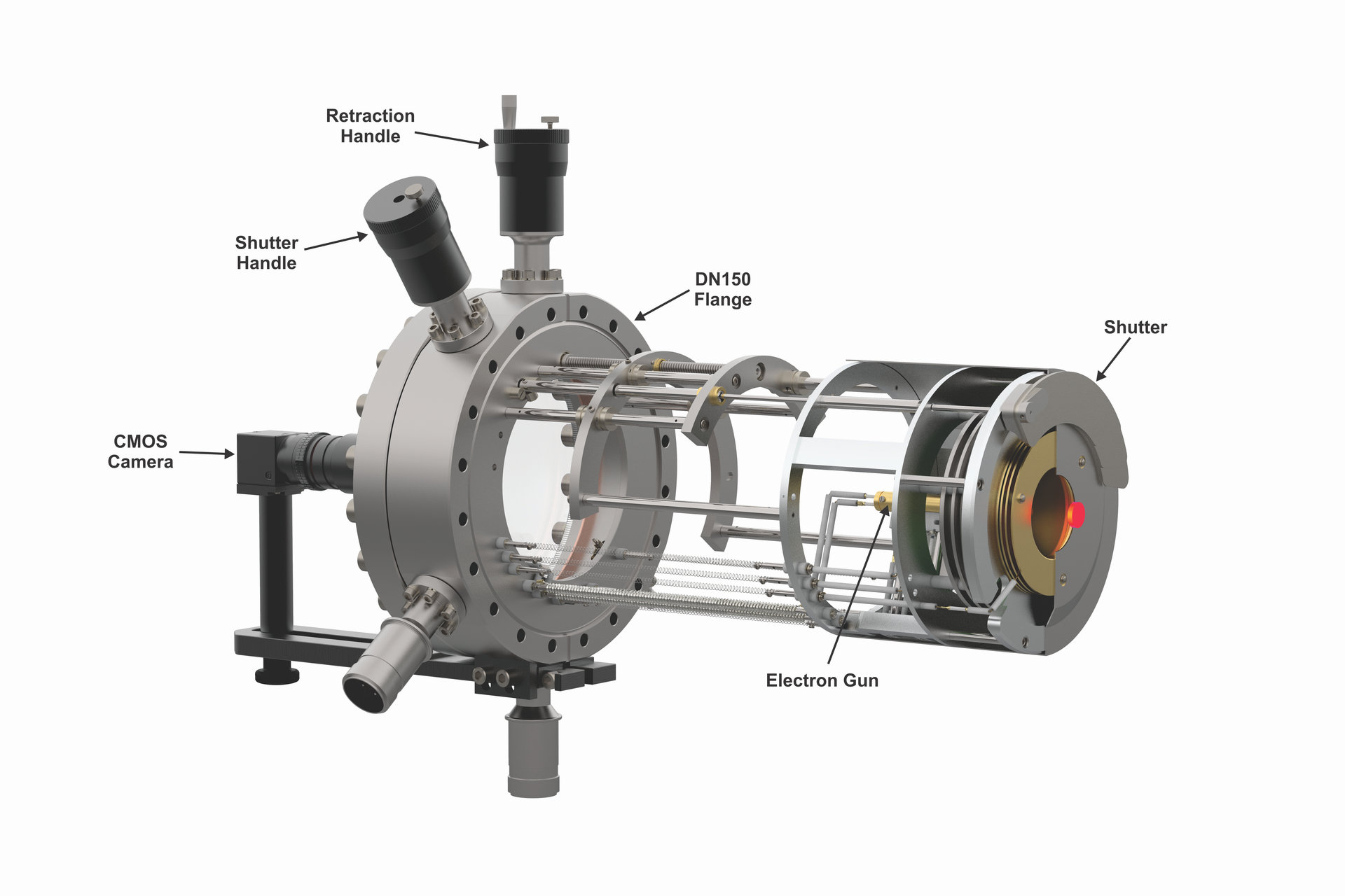 Figure 2. Model LPS075-D power supply for LEED operation.
  Figure 3. Model LPS300-D and LOA10-AES power supply for LEED and AES operation.
 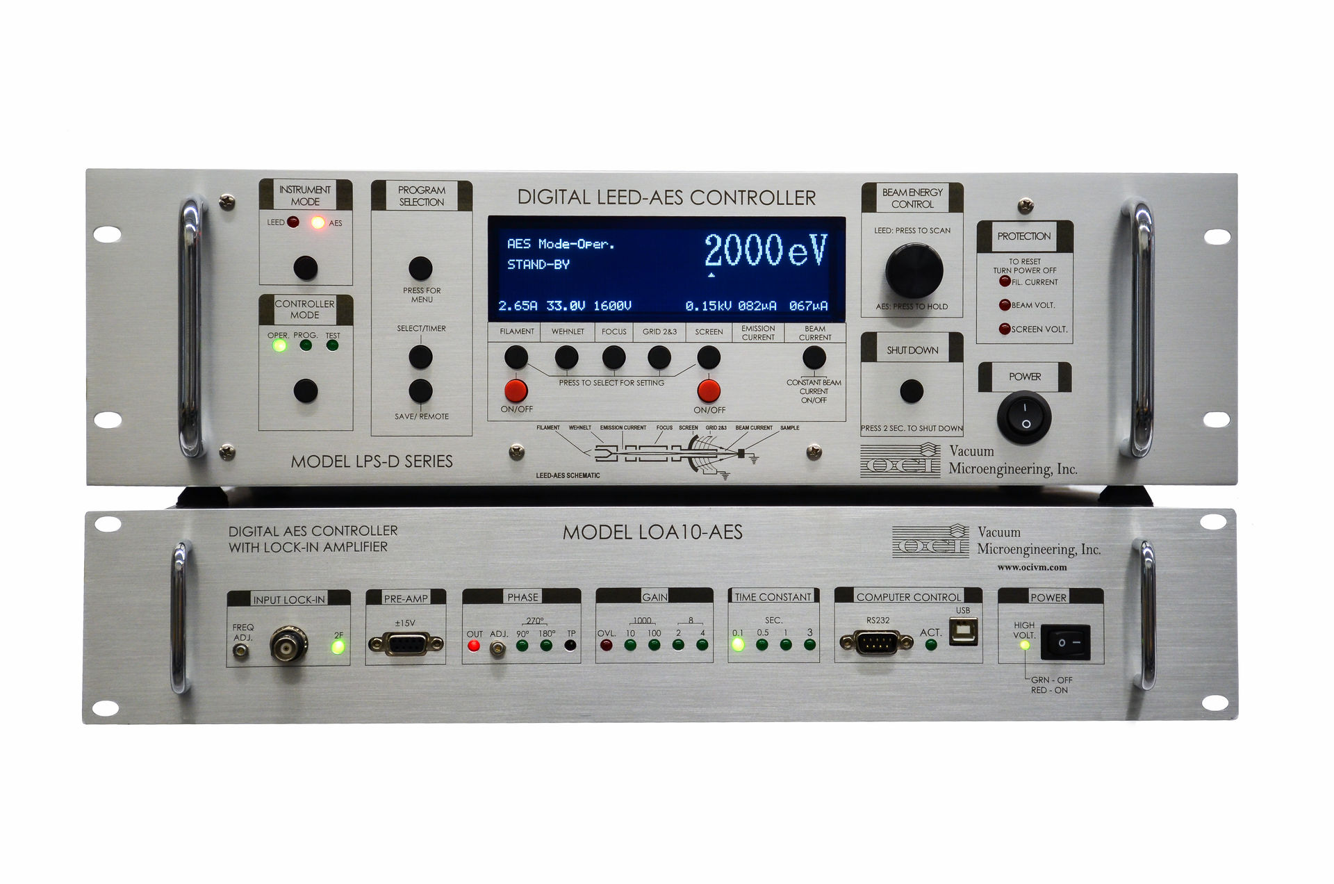 Figure 4. Model MCPS01/02 power supply for microchannel plate operation.
 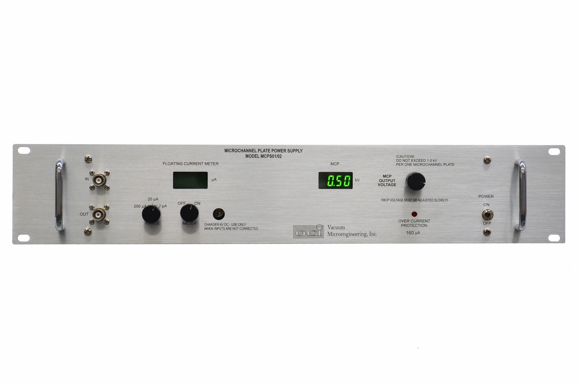 Figure 5. MultiLEED Software.
  Figure 6. AES Software.
  Figure 7. AES Software Images - element composition.
  Figure 8. LEED pattern of Germanium (100) with 120 eV beam energy.
 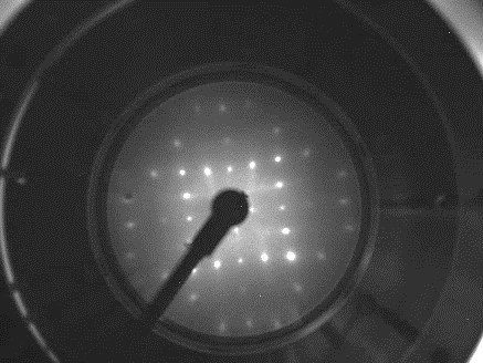 Figure 9. LEED pattern of Gallium Nitride (0001) with 64 eV beam energy.
 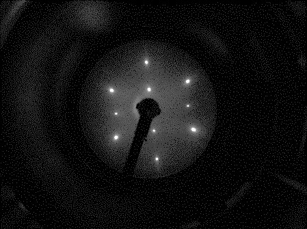 Figure 10. BP4 on Au (111) with 64 eV beam energy.
 -64eV.jpg) Figure 11. BP3 on Au (111) with 69 eV beam energy.
Figure 11. BP3 on Au (111) with 69 eV beam energy. -69eV.jpg) Figure 12. Auger spectrum of Gallium Nitride.
Figure 12. Auger spectrum of Gallium Nitride. 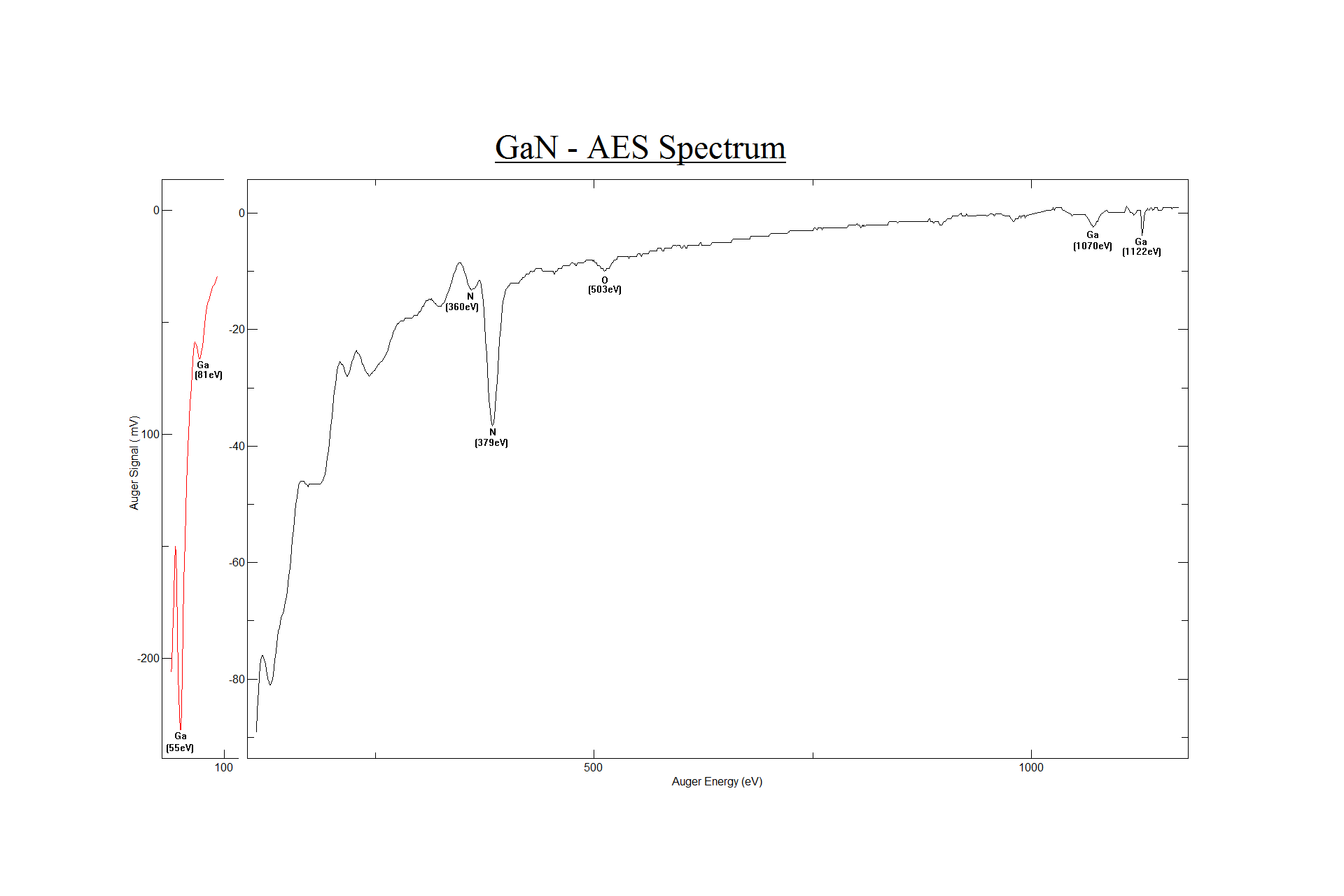 Figure 13. Auger spectrum of Gold.
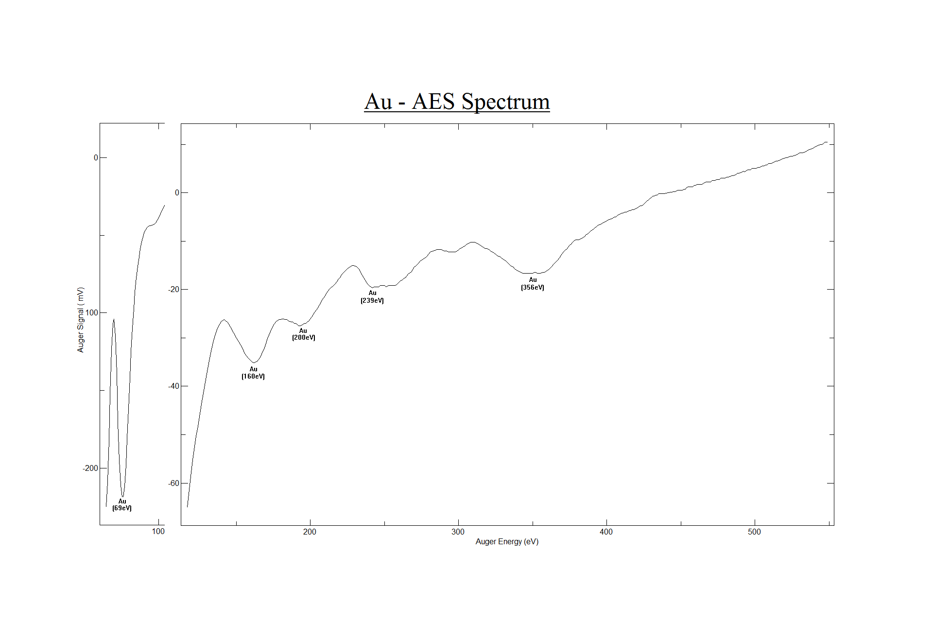
Description
The LEED 800 MCP-100DEG combines cutting-edge Low-Energy Electron Diffraction (LEED) and Auger Electron Spectroscopy (AES) capabilities with a wide viewing angle(100 °). Featuring a miniature electron gun, a set of concentric grids, and a conductive, phosphor-coated screen, and the superior signal amplification of single or dual microchannel plates (MCPs). The MCPs provide a high gain enabling the use of ultra-low beam currents to produce clear, high-resolution LEED patterns while minimizing sample damage—ideal for delicate materials like ice and organics.
Designed for ease of use, the The LEED 800 MCP-100DEG operates with a modern digital power supplies and a robust retraction mechanism, ensuring smooth, dependable day-to-day operation, as trusted by our extensive user base for decades. The wide viewing angle (100 ° at 33 mm sample distance) and minimal screen shadowing by the electron gun maximize the visible LEED pattern, providing unparalleled clarity and precision for surface science research.
Features
- High Image Sensitivity at the Primary Beam Current – 50 pA
- Single/Dual 75 mm Microchannel Plates
- AES at Beam Current 50 µA – 10 µA
- Large Angle (100°) Fluorescent LEED Display and superior magnetic shielding
- Miniature electron gun with large coherence width and dual lenses
- Suitable for ESDIAD
- Convenient LEED Image Capture with External Camera
- Simple and Powerful Operation with Digital Controller
Specifications, Configuration and More
IntegraLEED-Surface Crystallography Spectrometer
LEED 800 MCP (Model BDL800IR-MCP) w. Integral Retraction and Shutter
Organic Films & Molecular Beam Epitaxy
Based on Low Energy Electron Diffraction (LEED) and Auger Spectroscopy (AES)
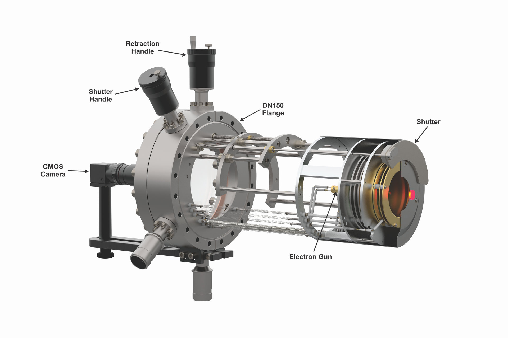 Figure 2. Model LPS075-D power supply for LEED operation.
Figure 3. Model LPS300-D and LOA10-AES power supply for LEED and AES operation.
Figure 4. Model MCPS01/02 power supply for microchannel plate operation.
Figure 5. MultiLEED Software.
Figure 6. AES Software.
Figure 7. AES Software Images - element composition.
Figure 8. LEED pattern of Germanium (100) with 120 eV beam energy.
Figure 9. LEED pattern of Gallium Nitride (0001) with 64 eV beam energy.
Figure 10. BP4 on Au (111) with 64 eV beam energy.
Figure 11. BP3 on Au (111) with 69 eV beam energy.
Figure 12. Auger spectrum of Gallium Nitride.
Figure 13. Auger spectrum of Gold.
Figure 2. Model LPS075-D power supply for LEED operation.
Figure 3. Model LPS300-D and LOA10-AES power supply for LEED and AES operation.
Figure 4. Model MCPS01/02 power supply for microchannel plate operation.
Figure 5. MultiLEED Software.
Figure 6. AES Software.
Figure 7. AES Software Images - element composition.
Figure 8. LEED pattern of Germanium (100) with 120 eV beam energy.
Figure 9. LEED pattern of Gallium Nitride (0001) with 64 eV beam energy.
Figure 10. BP4 on Au (111) with 64 eV beam energy.
Figure 11. BP3 on Au (111) with 69 eV beam energy.
Figure 12. Auger spectrum of Gallium Nitride.
Figure 13. Auger spectrum of Gold.
Description
The LEED 800 MCP combines cutting-edge Low-Energy Electron Diffraction (LEED) and Auger Electron Spectroscopy (AES) capabilities. Featuring a miniature electron gun, a set of concentric grids, and a conductive, phosphor-coated screen, and the superior signal amplification of single or dual microchannel plates (MCPs). The MCPs provide a high gain enabling the use of ultra-low beam currents to produce clear, high-resolution LEED patterns while minimizing sample damage—ideal for delicate materials like ice and organics.
Designed for ease of use, the LEED 800 MCP operates with a modern digital power supplies and a robust retraction mechanism, ensuring smooth, dependable day-to-day operation, as trusted by our extensive user base for decades. The wide viewing angle (78 ° at 50 mm sample distance) and minimal screen shadowing by the electron gun maximize the visible LEED pattern, providing unparalleled clarity and precision for surface science research.
Features
- High Image Sensitivity at the Primary Beam Current – 50 pA
- Single/Dual 75 mm Microchannel Plates
- AES at Beam Current 50 µA – 10 µA
- Large Angle (78°) Fluorescent LEED Display and superior magnetic shielding
- Miniature electron gun with large coherence width and dual lenses
- Suitable for ESDIAD
- Convenient LEED Image Capture with External Camera
- Simple and Powerful Operation with Digital Controller
Specifications, Configuration and More
IntegraLEED Surface Crystallography Spectrometer
LEED 600 MCP (Model BDL600IR-MCP) with Integral Retraction
Compact LEED for Organic Films & Molecular Beam Epitaxy
Based on Low Energy Electron Diffraction (LEED) and Auger Spectroscopy (AES)
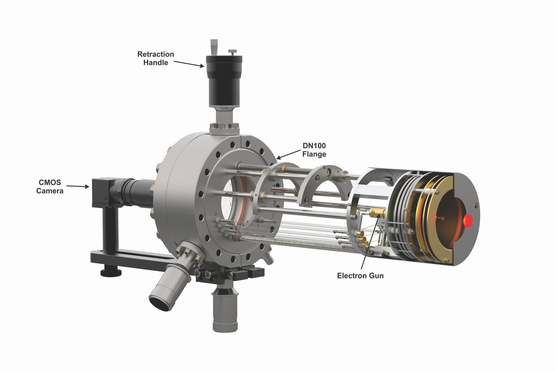 Figure 2. Model LPS075-D power supply for LEED operation.
  Figure 3. Model LPS300-D and LOA10-AES power supply for LEED and AES operation.
  Figure 4. Model MCPS01/02 power supply for microchannel plate operation.
  Figure 5. MultiLEED Software.
  Figure 6. AES Software.
  Figure 7. AES Software Images - element composition.
  Figure 8. LEED pattern of Silicon (111) with 80 eV beam energy.
 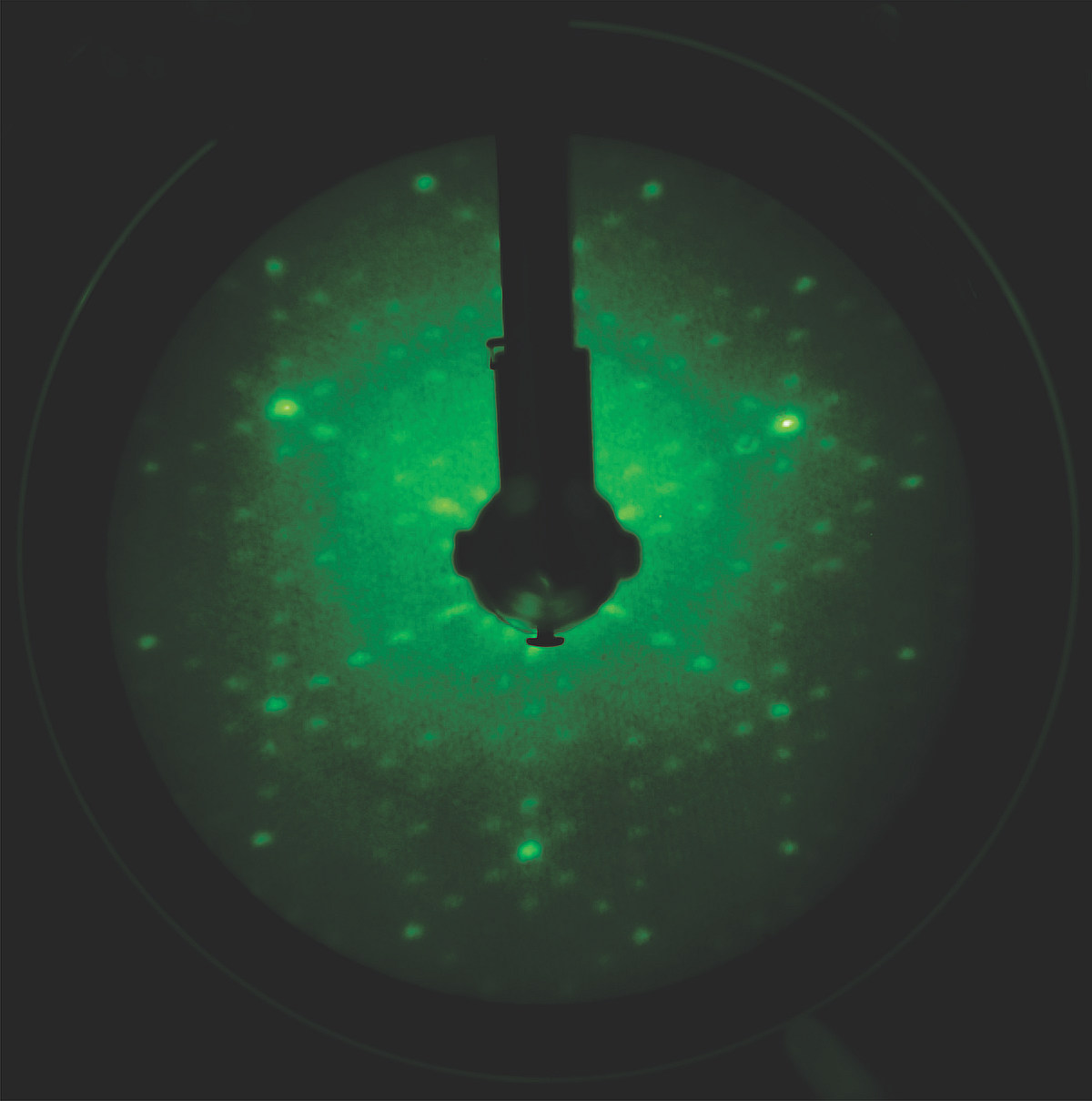 Figure 9. Auger spectrum of Silicon (111).
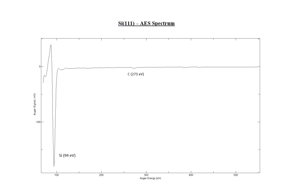
Description
The LEED 600 MCP combines cutting-edge Low-Energy Electron Diffraction (LEED) and Auger Electron Spectroscopy (AES) capabilities. Featuring a miniature electron gun, a set of concentric grids, and a conductive, phosphor-coated screen, and the superior signal amplification of single or dual microchannel plates (MCPs). The MCPs provide a high gain enabling the use of ultra-low beam currents to produce clear, high-resolution LEED patterns while minimizing sample damage—ideal for delicate materials like ice and organics.
Designed for ease of use, the LEED 600 MCP operates with a modern digital power supplies and a robust retraction mechanism, ensuring smooth, dependable day-to-day operation, as trusted by our extensive user base for decades. The wide viewing angle (71 ° at 49 mm sample distance) and minimal screen shadowing by the electron gun maximize the visible LEED pattern, providing unparalleled clarity and precision for surface science research.
Features
- High Image Sensitivity at the Primary Beam Current – 50 pA
- Single/Dual 75 mm Microchannel Plates
- AES at Beam Current 50 µA – 10 µA
- Large Angle (71°) Fluorescent LEED Display and superior magnetic shielding
- Miniature electron gun with large coherence width and dual lenses
- Suitable for ESDIAD
- Convenient LEED Image Capture with External Camera
- Simple and Powerful Operation with Digital Controller
Specifications, Configuration and More
IntegraLEED Surface Crystallography Spectrometer
LEED 450 MAX MCP (Model BDL450-MAX-MCP) with Integral Retraction and Shutter
Miniature Instrument to Fit Any UHV System
Upgraded version of the LEED450 featuring maximized display size for Surface crystallography.
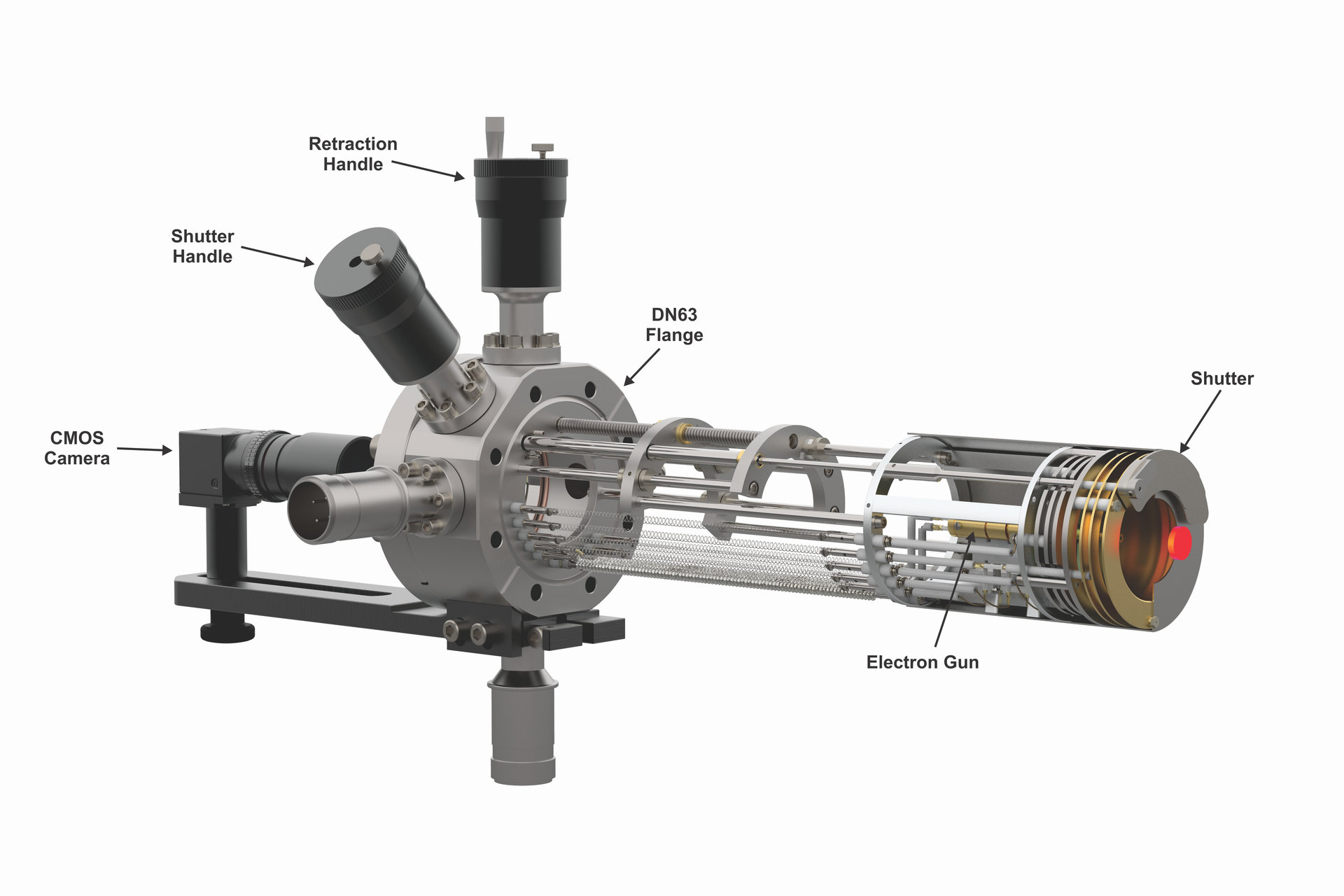 Figure 2. Model LPS075-D power supply for LEED operation.
Figure 3. Model LPS300-D and LOA10-AES power supply for LEED and AES operation.
Figure 4. Model MCPS01/02 power supply for microchannel plate operation.
Figure 5. MultiLEED Software.
Figure 6. AES Software.
Figure 7. AES Software Images - element composition.
Figure 8. LEED pattern of Germanium (100) with 120 eV beam energy.
Figure 9. LEED pattern of Gallium Nitride (0001) with 64 eV beam energy.
Figure 10. BP4 on Au (111) with 64 eV beam energy.
Figure 11. BP3 on Au (111) with 69 eV beam energy.
Figure 12. Auger spectrum of Gallium Nitride.
Figure 13. Auger spectrum of Gold.
Figure 2. Model LPS075-D power supply for LEED operation.
Figure 3. Model LPS300-D and LOA10-AES power supply for LEED and AES operation.
Figure 4. Model MCPS01/02 power supply for microchannel plate operation.
Figure 5. MultiLEED Software.
Figure 6. AES Software.
Figure 7. AES Software Images - element composition.
Figure 8. LEED pattern of Germanium (100) with 120 eV beam energy.
Figure 9. LEED pattern of Gallium Nitride (0001) with 64 eV beam energy.
Figure 10. BP4 on Au (111) with 64 eV beam energy.
Figure 11. BP3 on Au (111) with 69 eV beam energy.
Figure 12. Auger spectrum of Gallium Nitride.
Figure 13. Auger spectrum of Gold.
Description
The LEED 450-MAX-MCP combines cutting-edge Low-Energy Electron Diffraction (LEED) and Auger Electron Spectroscopy (AES) capabilities. Featuring a miniature electron gun, a set of concentric grids, and a conductive, phosphor-coated screen, and the superior signal amplification of single microchannel plates (MCP). The MCP provide a high gain enabling the use of ultra-low beam currents to produce clear, high-resolution LEED patterns while minimizing sample damage—ideal for delicate materials like ice and organics.
Designed for ease of use, the LEED 450-MAX-MCP operates with a modern digital power supplies and a robust retraction mechanism, ensuring smooth, dependable day-to-day operation, as trusted by our extensive user base for decades. The wide viewing angle (60 ° at 37 mm sample distance) and minimal screen shadowing by the electron gun maximize the visible LEED pattern, providing unparalleled clarity and precision for surface science research.
Features
- Sufficient angular and energy resolution to detect surface reconstructions and composition changes
- Miniature Electron Gun with double focusing
- Superior magnetic shielding
- Moiré pattern reduction
- Suitable for “in situ” growth monitoring
- Integral Linear Motion and Shutter
- Low Outgassing Rate
- Easy add-on AES
- Convenient LEED image Capture with external camera
- Simple and powerful operation with digital controller
Specifications, Configuration and More
FemtoLEED Models
FemtoLEED Spectrometer DLD L1000
Ultra-Sensitive and Insulating Film Crystallography
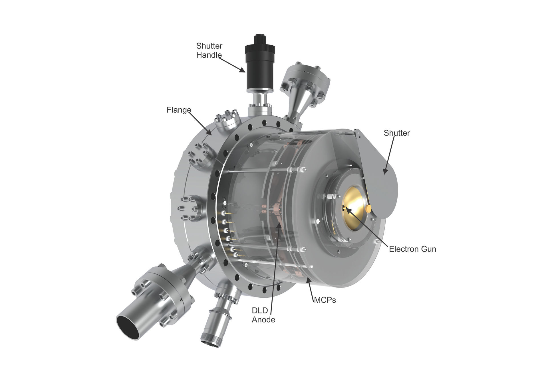 Figure 2. LPS-D power supply for LEED & microchannel plate power supply MCPS01/02.
 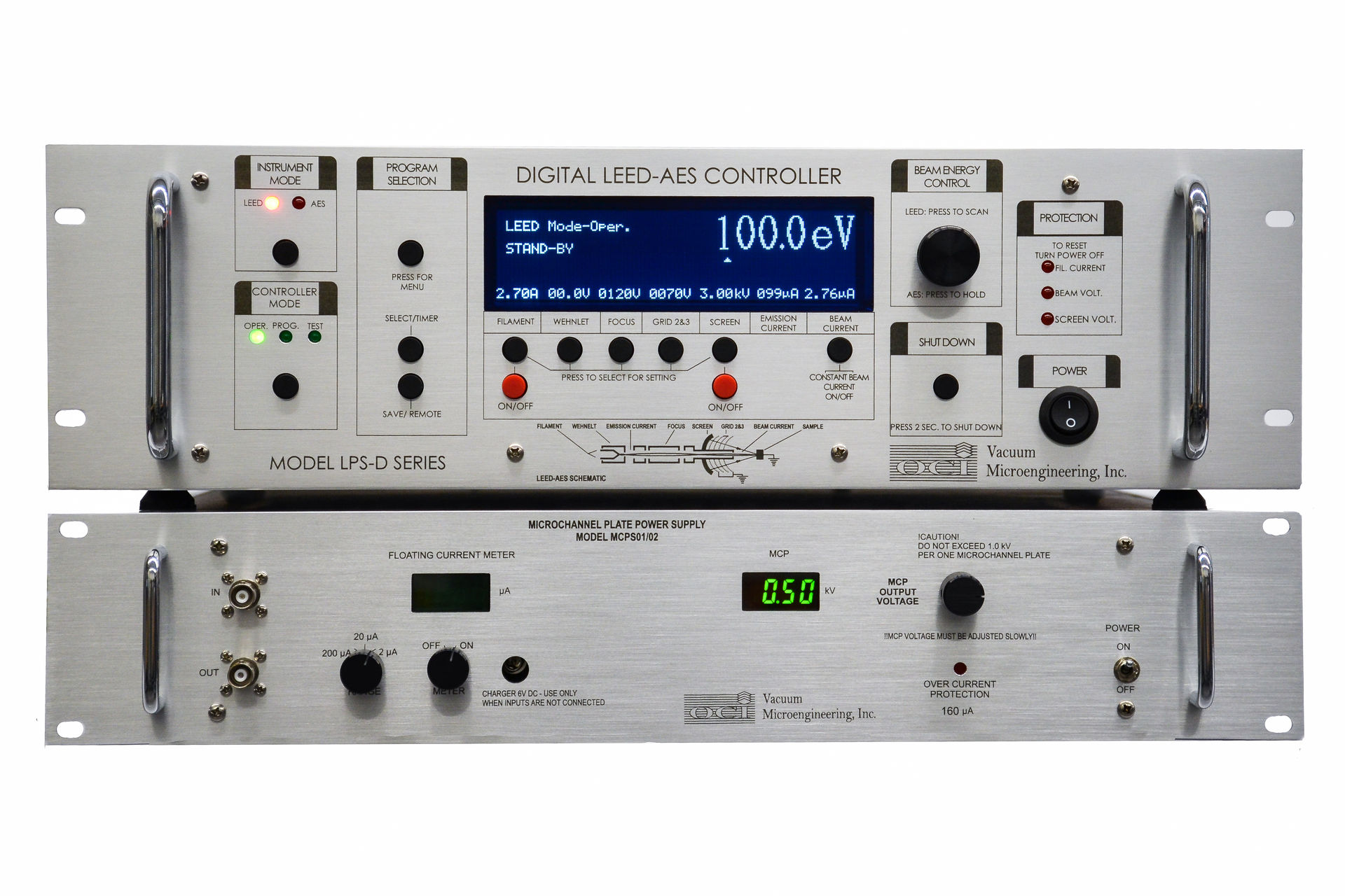 Figure 3. Silicon (111) with 35 eV beam energy.
 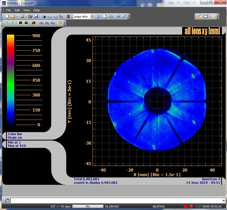 Figure 4. Silicon (111) with 140 eV beam energy.
 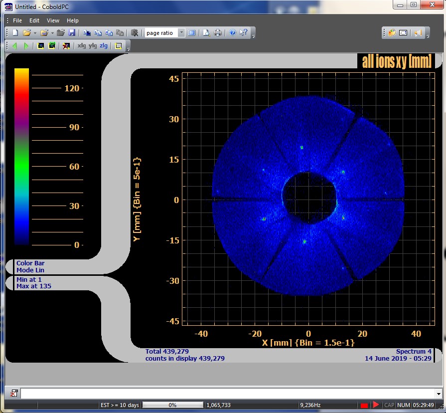 Figure 5. Germanium (001) with 136 eV beam energy.
 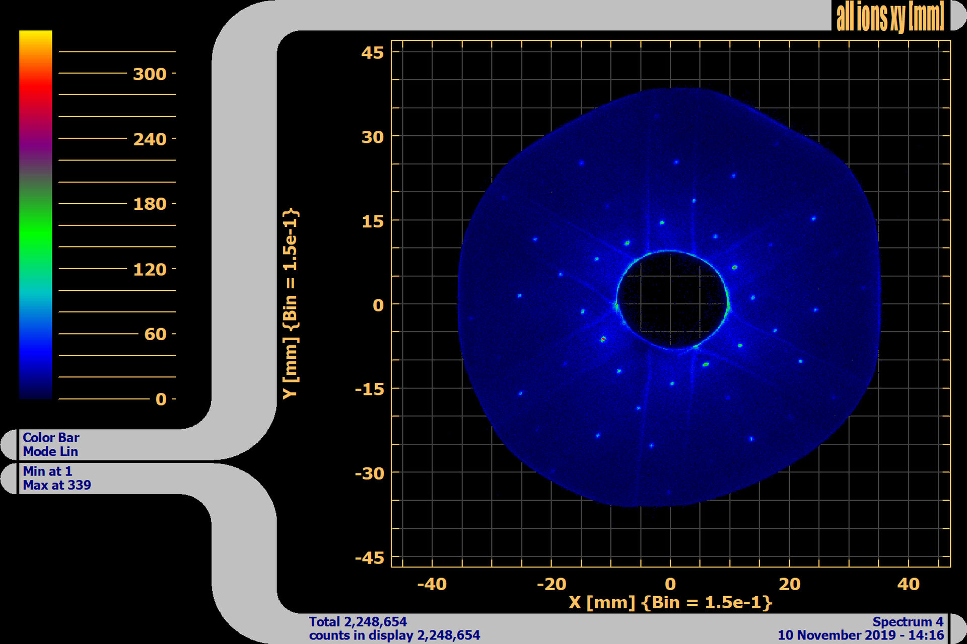 Figure 6. Germanium (001) with 200 eV beam energy.
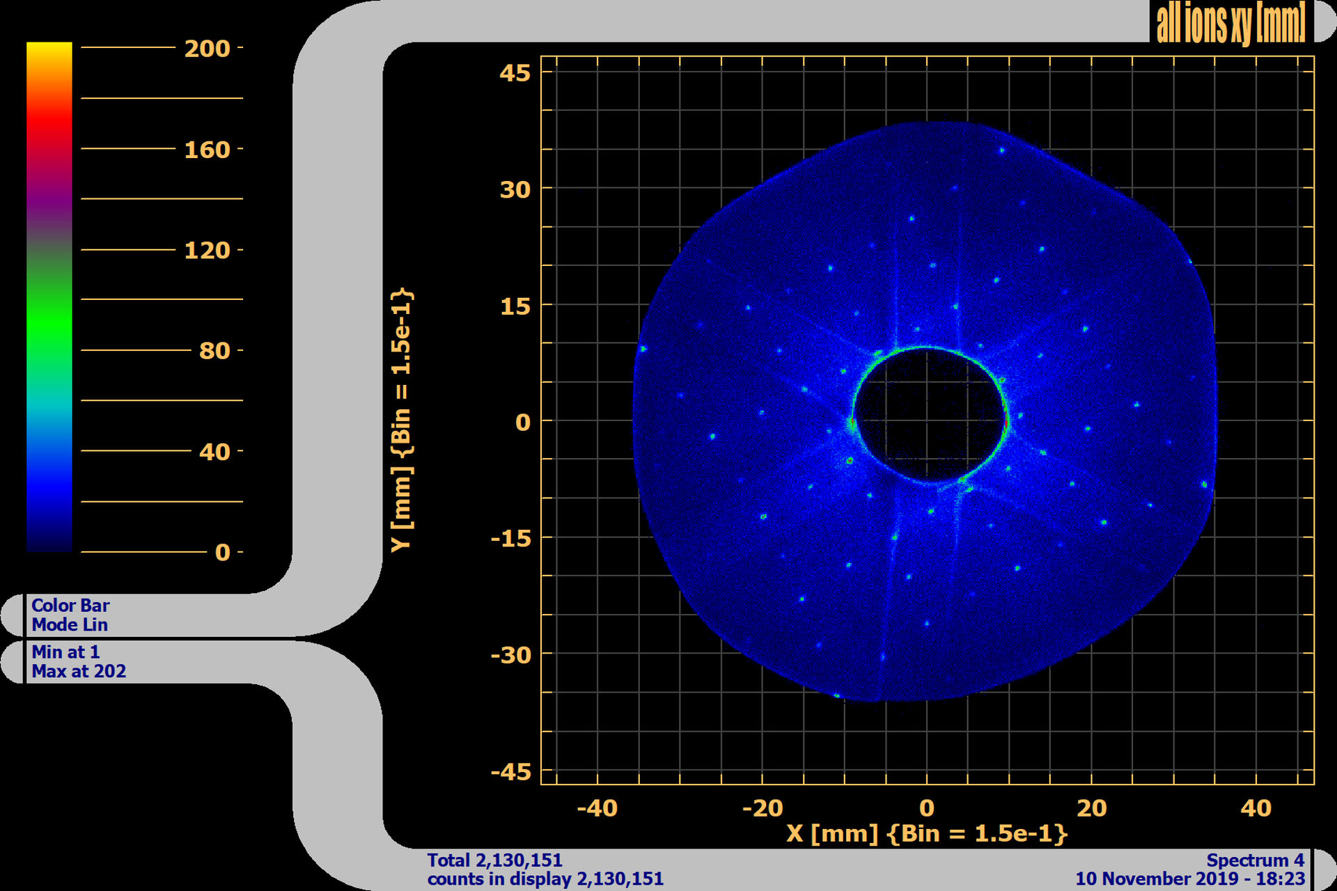
Collaboration with RoentDek in Germany. Notes:
Different electronics & software: LPS075-D (electron gun & grids); DLA-TR8 (controller for delay line detector & computer interface PCI card); DLD-LIM32 (delay line detector acquisition software & LEED analysis software for Windows 10/11); Cobold (for analyzing data from anode – hit times, location calculations etc. – to produce image).
In addition to the LPS075-D & MCPS02 controllers, a DLA-TR8 controller from RoentDek is needed for operation of the hexDLD-anode.
Description
The FemtoLEED DLD L1000 with integral shutter enables measurements of ultra-sensitive and insulating films. Instead of a fluorescent screen, it uses a delay line detector which allows for fully digital operation. The hex-anode provides minimized blind area due to the redundant detection opportunities of the added third delay line layer.
Features
- Fully digital
- Minimized blind area
- Electron diffraction on insulating single crystal samples
- Large coherence width
- Powerful operation with digital LEED controller
Specifications, Configuration and More
FemtoLEED Spectrometer DLD L800
Nano-Scale Measurements of Surface Periodic Structures with Femto-Ampere Electron Probe
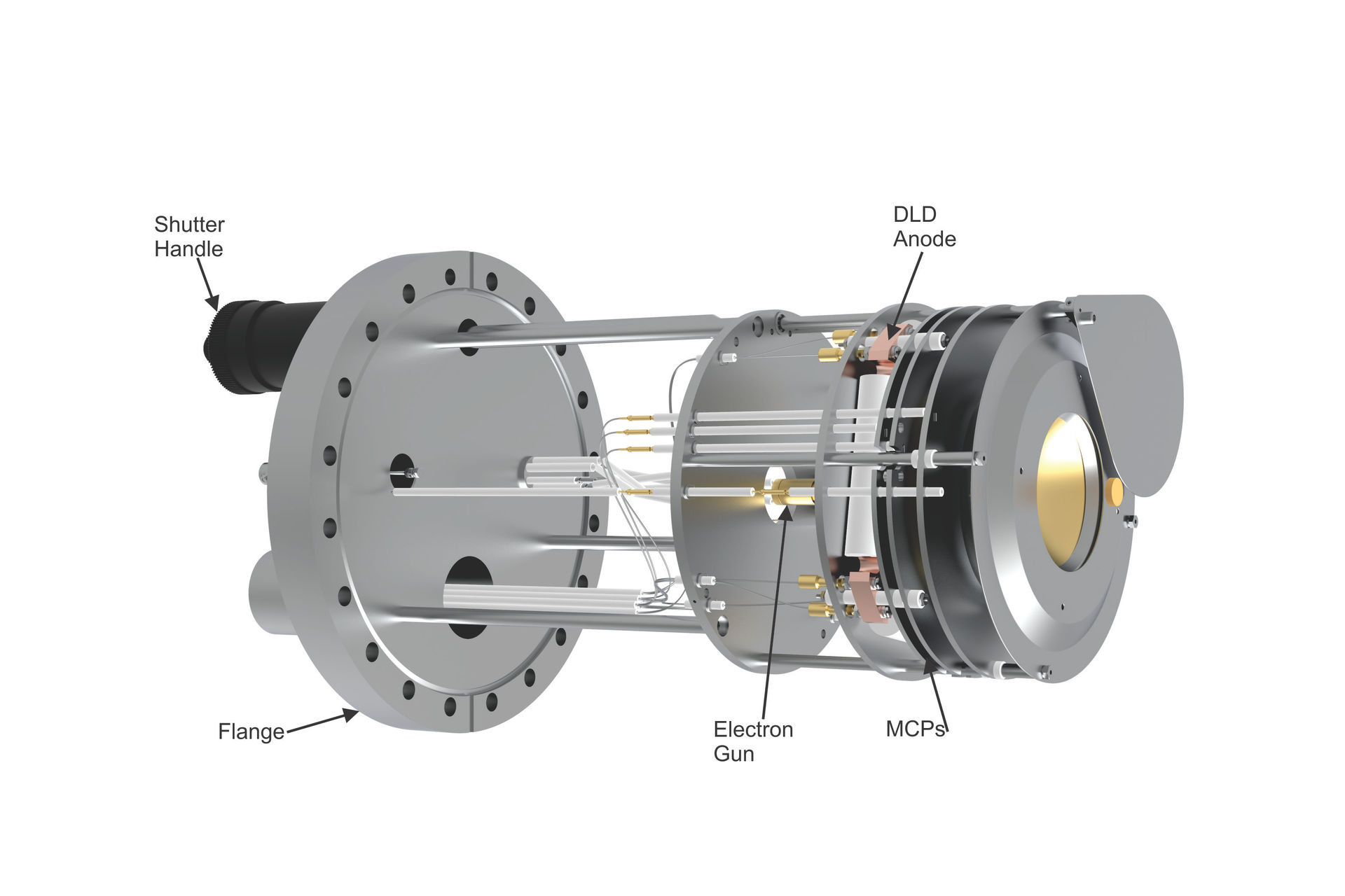 Figure 2. LPS-D power supply for LEED & microchannel plate power supply MCPS01/02.
Figure 4. Silicon (111) with 50 eV beam energy, 35 V GND.
Figure 2. LPS-D power supply for LEED & microchannel plate power supply MCPS01/02.
Figure 4. Silicon (111) with 50 eV beam energy, 35 V GND. 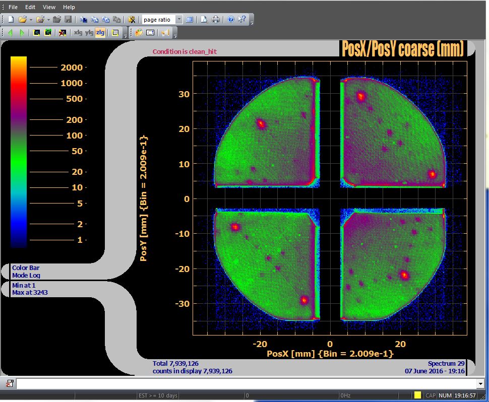 Figure 5. Silicon sample (185 deg) with 10 eV beam energy.
 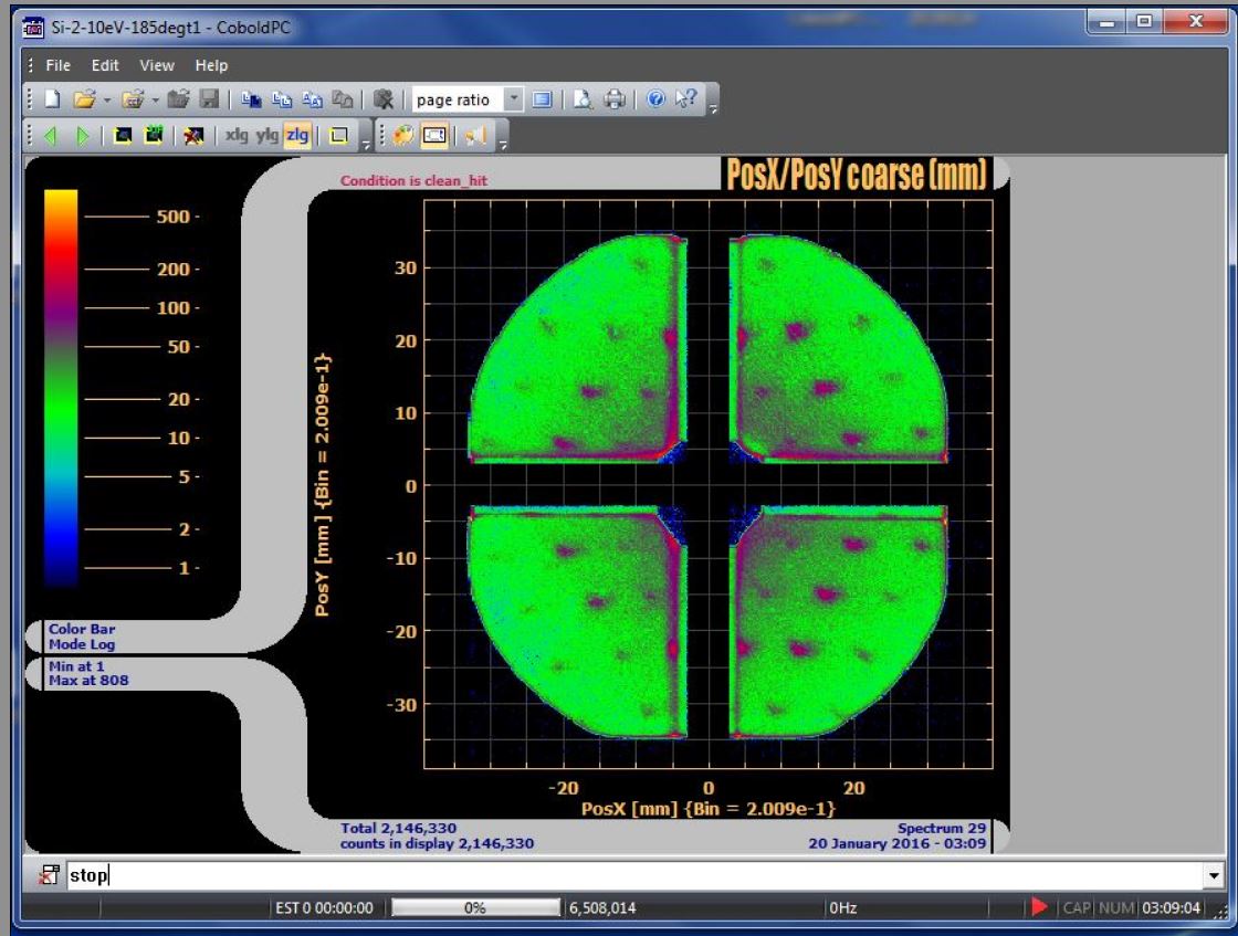 Figure 6. Magnesium Oxide sample.
 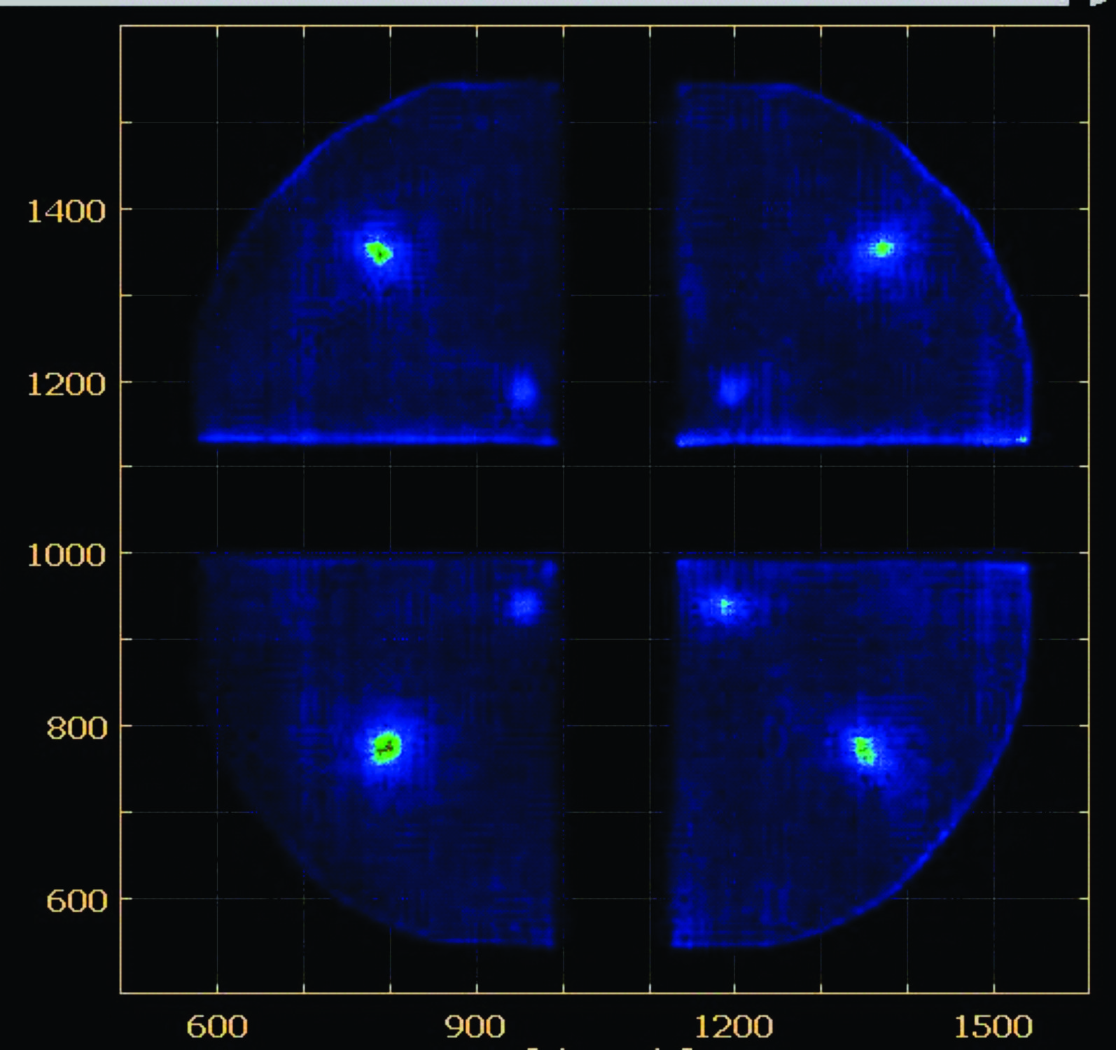 Figure 7. Magnesium Oxide (100) with 94 eV beam energy.
 -94eV.jpg)
Collaboration with RoentDek in Germany.
The FemtoLEED with integral shutter enables nano-scale measurements of surface periodic structures with a femto-ampere electron probe. Instead of a fluorescent screen, it uses a delay line detector and allows for fully digital operation.
Features
- Primary electron beam in the range of femto ampere
- Electron diffraction on insulating single crystal samples
- Large coherence width
- Powerful operation with digital LEED controller
Specifications, Configuration and More
AES Models
NDC600
Nano-Depth Composition Analyzer
Based on Auger Electron Spectroscopy (AES) Model NDC600
Description
Model NDC600 analyzer is the single stage cylindrical mirror analyzer (CMA) comprising of an axial miniature electron gun with robust tungsten filament. The energy resolution of the analyzer is 0.5 %. The signal detector is based on cylindrical slit followed by channel electron multiplier with gain greater than 3x10⁻⁷.
The high elemental sensitivity is achieved by combination of high gain - low noise Channeltron TM operated with sophisticated external bandpass filter for Auger signal processing. The Auger's signal detection is from 0.1 nm to 5 nm depth at the substrate surface.
Features
- High Surface Elemental Sensitivity
- Small Beam Size
- Suitable for Depth Profiling
- Adjustment for Sample Positioning & Retraction
- Compact Design